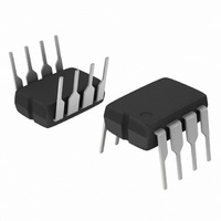
MC34063AP1G ON Semiconductor, MC34063AP1G Datasheet - Page 2

MC34063AP1G
Manufacturer Part Number
MC34063AP1G
Description
IC REG SW DC-DC INV 1.5A 8DIP
Manufacturer
ON Semiconductor
Type
Step-Down (Buck), Step-Up (Boost), Invertingr
Specifications of MC34063AP1G
Internal Switch(s)
Yes
Synchronous Rectifier
No
Number Of Outputs
1
Voltage - Output
1.25 ~ 40 V
Current - Output
1.5A
Frequency - Switching
100kHz
Voltage - Input
3 ~ 40 V
Operating Temperature
0°C ~ 70°C
Mounting Type
Through Hole
Package / Case
8-DIP (0.300", 7.62mm)
Power - Output
1.25W
Output Current
1.5 A
Input Voltage
3 V to 40 V
Switching Frequency
100 KHz
Operating Temperature Range
0 C to + 70 C
Mounting Style
Through Hole
Current, Input Bias
-20 nA
Current, Output
1.5 A
Current, Supply
4 mA
Frequency, Oscillator
33 kHz
Package Type
PDIP-8
Power Dissipation
1.25 W
Regulator Type
DC-DC, Switching
Temperature, Operating, Range
0 to +70 °C
Voltage, Input
-0.3 to +40 VDC
Voltage, Output
40 VDC
Voltage, Supply
40 VDC
Lead Free Status / RoHS Status
Lead free / RoHS Compliant
Other names
MC34063AP1GOS
Available stocks
Company
Part Number
Manufacturer
Quantity
Price
Company:
Part Number:
MC34063AP1G
Manufacturer:
ONSEMI
Quantity:
9 999
Part Number:
MC34063AP1G
Manufacturer:
ON/安森美
Quantity:
20 000
Stresses exceeding Maximum Ratings may damage the device. Maximum Ratings are stress ratings only. Functional operation above the
Recommended Operating Conditions is not implied. Extended exposure to stresses above the Recommended Operating Conditions may affect
device reliability.
1. Maximum package power dissipation limits must be observed.
2. This device series contains ESD protection and exceeds the following tests: Human Body Model 4000 V per MIL−STD−883, Method 3015.
3. NCV prefix is for automotive and other applications requiring site and change control.
MAXIMUM RATINGS
Power Supply Voltage
Comparator Input Voltage Range
Switch Collector Voltage
Switch Emitter Voltage (V
Switch Collector to Emitter Voltage
Driver Collector Voltage
Driver Collector Current (Note 1)
Switch Current
Power Dissipation and Thermal Characteristics
Operating Junction Temperature
Operating Ambient Temperature Range
Storage Temperature Range
Machine Model Method 400 V.
Plastic Package, P, P1 Suffix
SOIC Package, D Suffix
MC34063A
MC33063AV, NCV33063A
MC33063A
T
Thermal Resistance
T
Thermal Resistance
A
A
= 25°C
= 25°C
Pin 1
= 40 V)
Rating
MC34063A, MC33063A, NCV33063A
2
V
V
V
V
Symbol
I
CE(switch)
C(driver)
C(switch)
E(switch)
C(driver)
R
R
V
I
T
V
P
P
SW
T
T
qJA
qJA
stg
CC
IR
D
D
A
J
−40 to +125
−65 to +150
−0.3 to + 40
−40 to + 85
Value
0 to +70
+150
1.25
100
100
625
160
1.5
40
40
40
40
40
°C/W
°C/W
Unit
Vdc
Vdc
Vdc
Vdc
Vdc
Vdc
mW
mA
°C
°C
°C
W
A


