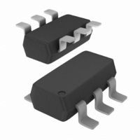
MAX1720EUTG ON Semiconductor, MAX1720EUTG Datasheet - Page 15

MAX1720EUTG
Manufacturer Part Number
MAX1720EUTG
Description
IC INVERTER CHRG PUMP VOLT 6TSOP
Manufacturer
ON Semiconductor
Type
Switched Capacitor (Charge Pump), Invertingr
Datasheet
1.MAX1720EUTG.pdf
(18 pages)
Specifications of MAX1720EUTG
Internal Switch(s)
Yes
Synchronous Rectifier
No
Number Of Outputs
1
Voltage - Output
-1.5 ~ -5.5 V, 3 ~ 11 V
Current - Output
50mA
Frequency - Switching
12kHz
Voltage - Input
1.5 ~ 5.5 V
Operating Temperature
-40°C ~ 85°C
Mounting Type
Surface Mount
Package / Case
SC-74-6
Power - Output
313mW
Function
Inverting
Output Voltage
- 5.5 V to - 1.15 V
Output Current
100 mA
Maximum Operating Temperature
+ 150 C
Mounting Style
SMD/SMT
Operating Supply Voltage (min)
1.15V
Operating Supply Voltage (max)
5.5V
Package Type
TSOP
Pin Count
6
Mounting
Surface Mount
Lead Free Status / RoHS Status
Lead free / RoHS Compliant
Other names
MAX1720EUTGOS
Available stocks
Company
Part Number
Manufacturer
Quantity
Price
Company:
Part Number:
MAX1720EUTG
Manufacturer:
ON Semiconductor
Quantity:
1 150
This is accomplished with the addition of two external switch transistors and two Schottky diodes. The output voltage is
approximately equal to 2V
The performance characteristics for the converter is shown below. Note that the output resistance is reduced to 1.9 W.
is connected to ground. This convert provides a line and load regulated output of 7.6 V at up to 300 mA with an input voltage
of 5.0 V. The output will regulate at a level of V
loop is the solid line. The performance characteristics are shown below.
The MAX1720 can be configured to produce a positive output voltage doubler with current capability in excess of 500 mA.
This converter is a combination of Figures 42 and the shunt regulator to close the loop. In this case the anode of the regulator
8.4
8.0
7.6
7.2
6.8
8.8
Figure 43. Positive Doubler with Current Boosted Load Regulation, Output Voltage vs. Output Current
0
Figure 44. Line and Load Regulated Positive Output Voltage Doubler with High Current Capability
Regulation, Output Voltage vs. Output Current
Figure 45. Current Boosted Close Loop Load
0.1
V
in
I
out
, OUTPUT CURRENT (A)
0.2
in
+
minus the sum of the base emitter drops of both transistors and the forward voltage of both diodes.
C
8.8
8.4
8.0
7.6
7.2
6.8
0.3
3
V
R
R
R
R
T
1
2
3
0
A
in
out
out
1
2
= 25°C
= 10 k
= 51.3 kW
= 5.0 V
= 1.9 W Open Loop
= 0.5 W Closed Loop
0.4
OSC
0.1
10 k
ref
I
out
0.5
(R
, OUTPUT CURRENT (A)
http://onsemi.com
0.2
2
6
5
4
/R
1
MAX1720
+ 1). The open loop configuration is the dashed line and the closed
0.6
15
0.3
50
50
8.0
7.0
6.0
5.0
4.0
3.0
2.0
1.0
1.0
Q
Q
0.4
2
1
Capacitors = 220 mF
Q
Q
Figure 46. Current Boosted Close Loop Line
Regulation, Output Voltage vs. Input Voltage
1
2
V
R
T
C
= PZT751
= PZT651
A
in
out
1
= 25°C
+
= 5.0 V
= 1.9 W
0.5
2.0
V
in
0.6
+
, INPUT VOLTGE (V)
3.0
C
2
R
R
1
2
4.0
V
I
R
R
T
out
out
A
1
2
= 25°C
= 10 k
= 51.3 kW
= 100 mA
5.0
6.0


