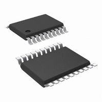
LM5005MH/NOPB National Semiconductor, LM5005MH/NOPB Datasheet - Page 18

LM5005MH/NOPB
Manufacturer Part Number
LM5005MH/NOPB
Description
IC BUCK SYNC ADJ 2.5A 20TSSOP
Manufacturer
National Semiconductor
Type
Step-Down (Buck)r
Datasheet
1.LM5005MHXNOPB.pdf
(22 pages)
Specifications of LM5005MH/NOPB
Internal Switch(s)
Yes
Synchronous Rectifier
No
Number Of Outputs
1
Voltage - Output
1.23 ~ 70 V
Current - Output
2.5A
Frequency - Switching
500kHz
Voltage - Input
7 ~ 75 V
Operating Temperature
-40°C ~ 125°C
Mounting Type
Surface Mount
Package / Case
20-TSSOP Exposed Pad, 20-eTSSOP, 20-HTSSOP
Power - Output
3.5W
Dc To Dc Converter Type
Inverting/Step Down
Pin Count
20
Input Voltage
75V
Output Voltage
1.225 to 70V
Switching Freq
50 TO 500KHz
Output Current
2.5A
Efficiency
90%
Package Type
TSSOP EP
Output Type
Adjustable
Switching Regulator
Yes
Mounting
Surface Mount
Input Voltage (min)
7V
Operating Temp Range
-40C to 125C
Operating Temperature Classification
Automotive
For Use With
LM5005EVAL - BOARD EVALUATION LM5005
Lead Free Status / RoHS Status
Lead free / RoHS Compliant
Other names
*LM5005MH
*LM5005MH/NOPB
LM5005MH
*LM5005MH/NOPB
LM5005MH
Available stocks
Company
Part Number
Manufacturer
Quantity
Price
Company:
Part Number:
LM5005MH/NOPB
Manufacturer:
TI
Quantity:
3 000
Part Number:
LM5005MH/NOPB
Manufacturer:
NS/国半
Quantity:
20 000
www.national.com
PWB BOARD LAYOUT AND THERMAL
CONSIDERATIONS
The circuit in Figure 1 serves as both a block diagram of the
LM5005 and a typical application board schematic for the
LM5005. In a buck regulator there are two loops where cur-
rents are switched very fast. The first loop starts from the input
capacitors, to the regulator VIN pin, to the regulator SW pin,
to the inductor then out to the load. The second loop starts
from the output capacitor ground, to the regulator PGND pins,
to the regulator IS pins, to the diode anode, to the inductor
and then out to the load. Minimizing the loop area of these
two loops reduces the stray inductance and minimizes noise
and possible erratic operation. A ground plane in the PC
board is recommended as a means to connect the input filter
capacitors to the output filter capacitors and the PGND pins
of the regulator. Connect all of the low power ground connec-
tions (C
Connect the AGND and PGND pins together through the top-
side copper area covering the entire underside of the device.
C
C
C
C
C
C
C
C
C
C
C
C
D
R
R
R
R
R
R
R
U
L
ITEM
SS
10
11
12
1
2
3
4
5
6
7
8
9
1
1
1
2
3
4
5
6
7
1
, R
T
, C
C4532X7R2A225M
C4532X7R2A225M
C0805C331G1GAC
C2012X7R2A103K
C2012X7R2A103K
OPEN
C2012X7R2A223K
C2012X7R1C474M
C3225X7R1C226M
EEFHE0J151R
C0805C331G1GAC
OPEN
CSHD6-100C
6CWQ10FN
DR127-330
OPEN
OPEN
CRCW08052102F
CRCW08054992F
CRCW08055111F
CRCW08051651F
CRCW2512100J
LM5005
RAMP
) directly to the regulator AGND pin.
PART NUMBER
TABLE 1. 5V, 2.5A Demo Board Bill of Materials
CAPACITOR, CER, TDK
CAPACITOR, CER, TDK
CAPACITOR, CER, KEMET
CAPACITOR, CER, TDK
CAPACITOR, CER, TDK
NOT USED
CAPACITOR, CER, TDK
CAPACITOR, CER, TDK
CAPACITOR, CER, TDK
CAPACITOR, SP, PANASINIC
CAPACITOR, CER, KEMET
NOT USED
DIODE, 100V, CENTRAL
DIODE, 100V, IR (D1-ALT)
INDUCTOR, COOPER
NOT USED
NOT USED
RESISTOR
RESISTOR
RESISTOR
RESISTOR
RESISTOR
REGULATOR, NATIONAL SEMICONDUCTOR
18
Place several vias in this underside copper area to the ground
plane.
The two highest power dissipating components are the re-
circulating diode and the LM5005 regulator IC. The easiest
method to determine the power dissipated within the LM5005
is to measure the total conversion losses (Pin – Pout) then
subtract the power losses in the Schottky diode, output in-
ductor and snubber resistor. An approximation for the Schot-
tky diode loss is P = (1-D) x Iout x Vfwd. An approximation for
the output inductor power is P = I
the DC resistance of the inductor and the 1.1 factor is an ap-
proximation for the ac losses. If a snubber is used, the power
loss can be estimated with an oscilloscope by observation of
the resistor voltage drop at both turn-on and turn-off transi-
tions. The regulator has an exposed thermal pad to aid power
dissipation. Adding several vias under the device to the
ground plane will greatly reduce the regulator junction tem-
perature. Selecting a diode with an exposed pad will aid the
power dissipation of the diode.
DESCRIPTION
OUT
2
x R x 1.1, where R is
0.022µ, 100V
0.01µ, 100V
0.01µ, 100V
330p, 100V
330p, 100V
2.2µ, 100V
2.2µ, 100V
0.47µ, 16V
150µ, 6.3V
22µ, 16V
VALUE
10, 1W
49.9K
5.11K
1.65K
33µH
21K


