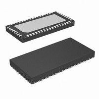
ISL65426HRZS2698 Intersil, ISL65426HRZS2698 Datasheet - Page 16

ISL65426HRZS2698
Manufacturer Part Number
ISL65426HRZS2698
Description
IC REG DUAL SYNC BUCK 6A 50-QFN
Manufacturer
Intersil
Type
Step-Down (Buck)r
Datasheet
1.ISL65426HRZ.pdf
(22 pages)
Specifications of ISL65426HRZS2698
Internal Switch(s)
Yes
Synchronous Rectifier
Yes
Number Of Outputs
2
Voltage - Output
1 ~ 4 V
Current - Output
6A
Frequency - Switching
1MHz
Voltage - Input
3 ~ 5.5 V
Operating Temperature
-10°C ~ 100°C
Mounting Type
Surface Mount
Package / Case
50-VQFN
Lead Free Status / RoHS Status
Lead free / RoHS Compliant
Power - Output
-
in Table 2. When each pin is pulled to GND by an internal
10µA pull-down, this default condition programs the output
voltage to the lowest level. The pull-down prevents situations
where a pin could be left floating for example (cold solder
joint) from causing the output voltage to rise above the
programmed level and damage a sensitive load device.
For designers requiring an output voltage level outside those
shown in Table 2, the ISL65426 allows user programming with
an external resistor divider (see Figure 36). First, both channel
selection pins associated with that output channel must be
tied to GND to set the internal reference to 0.6V. Next, the
output voltage is set by an external resistive divider according
to Equation 1. R
usually a good starting point. The designer can configure the
output voltage from 1V to 4V from a 5V power supply. Lower
input supply voltages reduce the maximum programmable
output voltage to 80% of the input voltage level.
Switching Frequency
The controller features an internal oscillator running at a
fixed frequency of 1MHz. The oscillator tolerance is +20%
over input bias and load range.
Operation Initialization
The ISL65426 initializes based on the state of three enable
inputs (EN, EN1, EN2) and power-on reset (POR) monitors
on VCC and PVINx inputs. Successful initialization of the
controller prompts a one time power block configuration
check. Verification of proper phase connections lead to a
soft-start interval. The controller begins slowly ramping the
output voltages based on the enable input states. Once the
commanded output voltage is within the proper window of
R
VOUT1
1
1.8V
1.5V
1.2V
FIGURE 36. EXTERNAL OUTPUT VOLTAGE SELECTION
=
R
2
TABLE 2. OUTPUT VOLTAGE PROGRAMMING
⋅
V
----------------------------------
V1SET1
ISL65426
OUT
0.6V
1
0
1
2
–
FB
LX
0.6V
is selected arbitrarily, but 5kΩ or 10kΩ is
V1SET2
EXTERNAL CONDITIONS
1
1
0
L
OUT
16
C
OUT
VOUT2
3.3V
2.5V
1.8V
R2
10kΩ
R1
13.3kΩ
V2SET1
V
1.4V
OUT
1
0
1
V2SET2
(EQ. 1)
1
1
0
ISL65426
operation, the power-good signal corresponding to the active
channel changes state from low to high indicating proper
operation initialization.
Power-On Reset
The POR circuitry prevents the controller from attempting to
soft-start before sufficient bias is present at vital power
supply input pins. These include the VCC and PVINx pins.
The VCC pins have a variable POR threshold based on the
output voltage configuration pin configuration of VOUT2. If
the configuration pins are set for 2.5V, the VCC POR rising
threshold is typically 2.9V. The 3.3V configuration increases
the VCC POR level to 4.3V. This variable rising threshold
guarantees that the controller can properly switch the
internal power blocks at the assigned output voltage levels.
The PVINx pins have a set POR rising threshold for all
output voltage configurations. While the voltage on these
pins are below this threshold (as defined in the “Electrical
Specifications” table), the controller inhibits switching of the
internal power MOSFETs.
Built-in hysteresis between the rising and falling thresholds
insures that once enabled, the controller will not
inadvertently toggle turn off unless the bias voltage drops
substantially. While these pins are below the POR rising
threshold, the synchronous power switch LX pins are held in
a high-impedance state.
If additional POR control is required, a system enable input
can be used to govern initialization, as described in the
following section.
Enable and Disable
If the POR input requirements are met, the ISL65426
remains in shutdown until the voltage at the enable inputs
rise above their enable thresholds. Independent enable
inputs, EN1 and EN2, allow initialization of either buck
converter channel separately, sequenced, or simultaneously.
Both pins feature a 10µA pull-up, which will initialize both
sides once the voltage at their respective pins exceeds the
rising enable threshold, as defined in the “Electrical
Specifications” table.
Both converters are governed by the presence of a system
enable, EN. When two separate input supplies are used for
each channel of power blocks or an external signal needs to
govern the power-up sequence, the system enable provides
a start-up sequencing mechanism.
The system enable features an internal 11µA pull-down,
which is only active when the voltage on the EN pin is below
the enable threshold. The current sink pulls the EN pin low.
As VCC2 rises, the enable level is not set exclusively by the
resistor divider from VCC2. With the current sink active, the
March 25, 2008
FN6340.3


