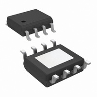
LM22672MR-ADJ/NOPB National Semiconductor, LM22672MR-ADJ/NOPB Datasheet - Page 10

LM22672MR-ADJ/NOPB
Manufacturer Part Number
LM22672MR-ADJ/NOPB
Description
IC REG SWITCH BUCK 1A ADJ 8PSOP
Manufacturer
National Semiconductor
Series
SIMPLE SWITCHER®r
Type
Step-Down (Buck)r
Specifications of LM22672MR-ADJ/NOPB
Internal Switch(s)
Yes
Synchronous Rectifier
No
Number Of Outputs
1
Voltage - Output
Adj to 1.285V
Current - Output
1A
Frequency - Switching
200kHz ~ 1MHz
Voltage - Input
4.5 ~ 42 V
Operating Temperature
-40°C ~ 125°C
Mounting Type
Surface Mount
Package / Case
8-PSOP
Dc To Dc Converter Type
Inverting/Step Down
Pin Count
8
Input Voltage
42V
Output Voltage
1.285V
Switching Freq
500/200 TO 1000KHz
Output Current
1A
Efficiency
90%
Package Type
PSOP EP
Output Type
Adjustable
Switching Regulator
Yes
Mounting
Surface Mount
Input Voltage (min)
4.5V
Operating Temperature Classification
Automotive
For Use With
551600236-001 - WEBENCH BUILD IT LM2267X 8-PSOPLM22672EVAL - BOARD EVALUATION FOR LM22672
Lead Free Status / RoHS Status
Lead free / RoHS Compliant
Power - Output
-
Lead Free Status / Rohs Status
Compliant
Other names
LM22672MR-ADJ
Available stocks
Company
Part Number
Manufacturer
Quantity
Price
Company:
Part Number:
LM22672MR-ADJ/NOPB
Manufacturer:
TI
Quantity:
16 700
Part Number:
LM22672MR-ADJ/NOPB
Manufacturer:
TI/德州仪器
Quantity:
20 000
www.national.com
Self Synchronize
It is also possible to self-synchronize multiple LM22672 reg-
ulators to share the same switching frequency. This can be
done by attaching the RT/SYNC pins together and putting a
1 kΩ resistor to ground. The diagram in
this setup. The two regulators will be clocked at the same fre-
quency but slightly phase shifted according to the minimum
off-time of the regulator with the fastest running oscillator. The
slight phase shift helps to reduce the stress on the input ca-
pacitors of the power supply.
Boot Pin
The LM22672 integrates an N-Channel FET switch and as-
sociated floating high voltage level shift / gate driver. This gate
driver circuit works in conjunction with an internal diode and
an external bootstrap capacitor. A 0.01 µF ceramic capacitor
connected with short traces between the BOOT pin and the
SW pin is recommended to effectively drive the internal FET
switch. During the off-time of the switch, the SW voltage is
approximately -0.5V and the external bootstrap capacitor is
charged from the internal supply through the internal boot-
strap diode. When operating with a high PWM duty-cycle, the
buck switch will be forced off each cycle to ensure that the
bootstrap capacitor is recharged. See the maximum duty-cy-
cle section for more details.
FIGURE 3. Switching Frequency vs RT/SYNC Resistor
FIGURE 4. Self Synchronizing Setup
30076730
Figure 4
30076713
illustrates
10
Thermal Protection
Internal Thermal Shutdown circuitry protects the LM22672 in
the event the maximum junction temperature is exceeded.
When activated, typically at 150°C, the regulator is forced into
a low power reset state. There is a typical hysteresis of 15
degrees.
Internal Compensation
The LM22672 has internal compensation designed for a sta-
ble loop with a wide range of external power stage compo-
nents.
Insuring stability of a design with a specific power stage (in-
ductor and output capacitor) can be tricky. The LM22672
stability can be verified over varying loads and input and out-
put voltages using WEBENCH® Designer online circuit sim-
ulation tool at www.national.com. A quick start spreadsheet
can also be downloaded from the online product folder.
The internal compensation of the -ADJ option of the LM22672
is optimized for output voltages below 5V. If an output voltage
of 5V or higher is needed, the -5.0 option with an additional
external resistor divider may also be used.
The typical location of the internal compensation poles and
zeros as well as the DC gain is given in
has internal type III compensation allowing for the use of most
output capacitors including ceramics.
This information can be used to calculate the transfer function
from the FB pin to the internal compensation node (input to
the PWM comparator in the block diagram).
For the power stage transfer function the standard voltage
mode formulas for the double pole and the ESR zero apply:
The peak ramp level of the oscillator signal feeding into the
PWM comparator is V
this modulator stage of the IC. The -5.0 fixed output voltage
option has twice the gain of the compensation transfer func-
tion compared to the -ADJ option which is 43.5dB instead of
37.5dB.
Generally, calculation as well as simulation can only aid in
selecting good power stage components. A good design prac-
tice is to test for stability with load transient tests or loop
measurement tests. Application note AN-1889 shows how to
easily perform a loop transfer function measurement with only
an oscilloscope and a function generator.
Corners
DC gain
Zero 1
Zero 2
Pole 1
Pole 2
Pole 3
IN
/10 which equals a gain of 20dB of
TABLE 1.
Table
Frequency
150 kHz
250 kHz
37.5 dB
1.5 kHz
100 Hz
15 kHz
1. The LM22672


