LM2596SX-ADJ/NOPB National Semiconductor, LM2596SX-ADJ/NOPB Datasheet - Page 3
LM2596SX-ADJ/NOPB
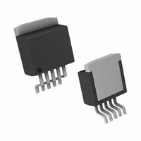
Manufacturer Part Number
LM2596SX-ADJ/NOPB
Description
IC REG SW ADJ 3A STP DN TO-263-5
Manufacturer
National Semiconductor
Series
SIMPLE SWITCHER®r
Type
Step-Down (Buck)r
Datasheet
1.LM2596S-ADJNOPB.pdf
(31 pages)
Specifications of LM2596SX-ADJ/NOPB
Internal Switch(s)
Yes
Synchronous Rectifier
No
Number Of Outputs
1
Voltage - Output
1.2 ~ 37 V
Current - Output
3A
Frequency - Switching
150kHz
Voltage - Input
4.5 ~ 40 V
Operating Temperature
-40°C ~ 125°C
Mounting Type
Surface Mount
Package / Case
D²Pak, TO-263 (5 leads + tab)
Primary Input Voltage
40V
No. Of Outputs
1
Output Voltage
37V
Output Current
3A
No. Of Pins
5
Operating Temperature Range
-40°C To +125°C
Msl
MSL 3 - 168 Hours
Filter Terminals
SMD
Rohs Compliant
Yes
Lead Free Status / RoHS Status
Lead free / RoHS Compliant
Power - Output
-
Other names
*LM2596SX-ADJ
*LM2596SX-ADJ/NOPB
LM2596SX-ADJ
*LM2596SX-ADJ/NOPB
LM2596SX-ADJ
Available stocks
Company
Part Number
Manufacturer
Quantity
Price

Part Number:
LM2596SX-ADJ/NOPB
Manufacturer:
TI/德州仪器
Quantity:
20 000


SYSTEM PARAMETERS (Note 5) Test Circuit Figure 1
V
SYSTEM PARAMETERS (Note 5) Test Circuit Figure 1
V
SYSTEM PARAMETERS (Note 5) Test Circuit Figure 1
V
OUT
OUT
OUT
Absolute Maximum Ratings
If Military/Aerospace specified devices are required,
please contact the National Semiconductor Sales Office/
Distributors for availability and specifications.
LM2596-3.3
Electrical Characteristics
Specifications with standard type face are for T
ture Range
LM2596-5.0
Electrical Characteristics
Specifications with standard type face are for T
ture Range
LM2596-12
Electrical Characteristics
Specifications with standard type face are for T
ture Range
Symbol
Symbol
Symbol
Maximum Supply Voltage
ON /OFF Pin Input Voltage
Feedback Pin Voltage
Output Voltage to Ground
Power Dissipation
Storage Temperature Range
ESD Susceptibility
(Steady State)
Output Voltage
Efficiency
Output Voltage
Efficiency
Output Voltage
Efficiency
Parameter
Parameter
Parameter
4.75V
V
7V
V
15V
V
IN
IN
IN
= 12V, I
= 12V, I
= 25V, I
V
V
IN
−65˚C to +150˚C
−0.3
IN
Internally limited
V
−0.3
IN
40V, 0.2A
LOAD
LOAD
LOAD
40V, 0.2A
J
J
J
(Note 1)
40V, 0.2A
V
= 25˚C, and those with boldface type apply over full Operating Tempera-
= 25˚C, and those with boldface type apply over full Operating Tempera-
= 25˚C, and those with boldface type apply over full Operating Tempera-
V +25V
Conditions
Conditions
Conditions
= 3A
= 3A
= 3A
+25V
−1V
45V
I
LOAD
I
LOAD
I
LOAD
3
3A
Operating Conditions
3A
Temperature Range
Supply Voltage
Lead Temperature
S Package
T Package (Soldering, 10 sec.)
Maximum Junction Temperature
3A
Human Body Model (Note 2)
Vapor Phase (60 sec.)
Infrared (10 sec.)
(Note 3)
(Note 3)
(Note 3)
12.0
Typ
Typ
Typ
3.3
5.0
73
80
90
LM2596-3.3
LM2596-5.0
LM2596-12
3.168/3.135
3.432/3.465
4.800/4.750
5.200/5.250
11.52/11.40
12.48/12.60
(Note 4)
(Note 4)
(Note 4)
Limit
Limit
Limit
−40˚C
T
4.5V to 40V
J
www.national.com
(Limits)
(Limits)
(Limits)
+215˚C
+245˚C
+260˚C
+150˚C
+125˚C
V(max)
V(max)
V(max)
V(min)
V(min)
V(min)
Units
Units
Units
2 kV
%
%
%
V
V
V
Related parts for LM2596SX-ADJ/NOPB
Image
Part Number
Description
Manufacturer
Datasheet
Request
R

Part Number:
Description:
Manufacturer:
National Semiconductor
Datasheet:
Part Number:
Description:
Manufacturer:
National Semiconductor
Datasheet:
Part Number:
Description:
Manufacturer:
National Semiconductor
Datasheet:
Part Number:
Description:
Manufacturer:
National Semiconductor
Datasheet:

Part Number:
Description:
IC REG SIMPLE SWITCHER TO-263-5
Manufacturer:
National Semiconductor
Datasheet:
Part Number:
Description:
IC REG SW 12V 3A STP DN TO-263-5
Manufacturer:
National Semiconductor
Datasheet:
Part Number:
Description:
IC REG SW 3.3V 3A STP DN TO263-5
Manufacturer:
National Semiconductor
Datasheet:

Part Number:
Description:
IC, STEP-DOWN VOLT REGULATOR 5V TO-220-5
Manufacturer:
National Semiconductor
Datasheet:
Part Number:
Description:
IC,SMPS CONTROLLER,VOLTAGE-MODE,BIPOLAR,SIP,5PIN,PLASTIC
Manufacturer:
National Semiconductor
Datasheet:
Part Number:
Description:
IC,SMPS CONTROLLER,VOLTAGE-MODE,BIPOLAR,SIP,5PIN,PLASTIC
Manufacturer:
National Semiconductor
Datasheet:

Part Number:
Description:
Simple Switcher Power Converter 150 Khz 3a Step-down Voltage Regulator
Manufacturer:
National Semiconductor Corporation
Datasheet:
Part Number:
Description:
IC REG SIMPLE SWITCHER TO-263-5
Manufacturer:
National Semiconductor
Datasheet:
Part Number:
Description:
IC REG SIMPLE SWITCHER TO-263-5
Manufacturer:
National Semiconductor
Datasheet:
Part Number:
Description:
IC REG SIMPLE SWITCHER TO-263-5
Manufacturer:
National Semiconductor
Datasheet:
Part Number:
Description:
IC REG SIMPLE SWITCHER TO-263-5
Manufacturer:
National Semiconductor
Datasheet: