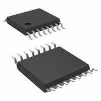
LM2854MHX-1000/NOPB National Semiconductor, LM2854MHX-1000/NOPB Datasheet - Page 14

LM2854MHX-1000/NOPB
Manufacturer Part Number
LM2854MHX-1000/NOPB
Description
IC REG 4A SYNC S SWITCH 16ETSSOP
Manufacturer
National Semiconductor
Series
PowerWise®, SIMPLE SWITCHER®r
Type
Step-Down (Buck)r
Datasheet
1.LM2854MH-1000NOPB.pdf
(22 pages)
Specifications of LM2854MHX-1000/NOPB
Internal Switch(s)
Yes
Synchronous Rectifier
Yes
Number Of Outputs
1
Voltage - Output
0.8 ~ 5 V
Current - Output
4A
Frequency - Switching
1MHz
Voltage - Input
2.95 ~ 5.5 V
Operating Temperature
-40°C ~ 125°C
Mounting Type
Surface Mount
Package / Case
16-TSSOP Exposed Pad, 16-eTSSOP, 16-HTSSOP
Lead Free Status / RoHS Status
Lead free / RoHS Compliant
Power - Output
-
Other names
LM2854MHX-1000
www.national.com
ENABLE AND UVLO
Using a resistor divider from VIN to EN as shown in the
schematic diagram below, the input voltage at which the part
begins switching can be increased above the normal input
UVLO level according to
For example, suppose that the required input UVLO level is
3.69V. Choosing R
kΩ.
Alternatively, the EN pin can be driven from another voltage
source to cater for system sequencing requirements com-
monly found in FPGA and other multi-rail applications. The
following schematic shows an LM2854 that is sequenced to
start based on the voltage level of a master system rail.
OUTPUT VOLTAGE SETTING
A divider resistor network from V
the desired output voltage as follows
EN2
= 10 kΩ, then we calculate R
OUT
to the FB pin determines
30052844
30052861
EN1
= 20
30052845
14
R
R
resistors are normally selected as 0.5% or 1% tolerance.
COMPENSATION COMPONENT SELECTION
The power stage transfer function of a voltage mode buck
converter has a complex double pole related to the LC output
filter and a left half plane zero due to the output capacitor
ESR, denoted R
given respectively by
where C
ated for applied voltage and operating temperature, R
effective load resistance and R
sistance associated with the inductor and power switches.
The conventional compensation strategy employed with volt-
age mode control is to use two compensator zeros to offset
the LC double pole, one compensator pole located to cancel
the output capacitor ESR zero and one compensator pole lo-
cated between one third and one half switching frequency for
high frequency noise attenuation.
The LM2854 internal compensation components are de-
signed to locate a pole at the origin and a pole at high
frequency as mentioned above. Furthermore, a zero is locat-
ed at 8.8 kHz or 17.6 kHz for the 500 kHz or 1 MHz options,
respectively, to approximately cancel the likely location of one
LC filter pole.
The three external compensation components, R
and C
pole location and a pole to cancel the ESR zero. The voltage
loop crossover frequency, f
one tenth to one fifth of the switching frequency
A simple solution for the required external compensation ca-
pacitor, C
expressed as
FB1
FB2
is defined based on the voltage loop requirements and
is then selected for the desired output voltage. These
COMP
O
COMP
is the output capacitance value appropriately der-
, are selected to position a zero at or below the LC
, with type III voltage mode control can be
ESR
0.1f
. The locations of these singularities are
SW
≤
loop
f
loop
, is usually selected between
DCR
≤
0.2f
is the series damping re-
SW
FB1
, R
L
is the
COMP
30052848


