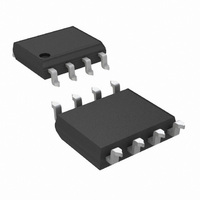
LM2675MX-5.0/NOPB National Semiconductor, LM2675MX-5.0/NOPB Datasheet - Page 22

LM2675MX-5.0/NOPB
Manufacturer Part Number
LM2675MX-5.0/NOPB
Description
IC REG SW 5V 1A STP DN 8-SOIC
Manufacturer
National Semiconductor
Series
SIMPLE SWITCHER®r
Type
Step-Down (Buck)r
Datasheet
1.LM2675LD-5.0.pdf
(26 pages)
Specifications of LM2675MX-5.0/NOPB
Internal Switch(s)
Yes
Synchronous Rectifier
No
Number Of Outputs
1
Voltage - Output
5V
Current - Output
1A
Frequency - Switching
260kHz
Voltage - Input
6.5 ~ 40 V
Operating Temperature
-40°C ~ 125°C
Mounting Type
Surface Mount
Package / Case
8-SOIC (3.9mm Width)
Dc To Dc Converter Type
Step Down
Pin Count
8
Input Voltage
40V
Output Voltage
5V
Switching Freq
260kHz
Output Current
1A
Efficiency
90%
Package Type
SOIC N
Output Type
Fixed
Switching Regulator
Yes
Mounting
Surface Mount
Input Voltage (min)
8V
Operating Temperature Classification
Automotive
Primary Input Voltage
12V
No. Of Outputs
1
No. Of Pins
8
Operating Temperature Range
-40°C To +125°C
Filter Terminals
SMD
Input Voltage Primary Max
40V
Rohs Compliant
Yes
For Use With
LM2675-5.0EVAL - EVALUATION BOARD FOR LM2675-5.0
Lead Free Status / RoHS Status
Lead free / RoHS Compliant
Power - Output
-
Lead Free Status / Rohs Status
Compliant
Other names
*LM2675MX-5.0
*LM2675MX-5.0/NOPB
LM2675MX-5.0
*LM2675MX-5.0/NOPB
LM2675MX-5.0
Available stocks
Company
Part Number
Manufacturer
Quantity
Price
Part Number:
LM2675MX-5.0/NOPB
Manufacturer:
TI/德州仪器
Quantity:
20 000
www.national.com
Application Information
TYPICAL SURFACE MOUNT PC BOARD LAYOUT,
FIXED OUTPUT (4X SIZE)
C
C
D1 - 1A, 40V Schottky Rectifier, Surface Mount
L1 - 33 µH, L23, Coilcraft DO3316
C
TYPICAL SURFACE MOUNT PC BOARD LAYOUT,
ADJUSTABLE OUTPUT (4X SIZE)
C
C
D1 - 1A, 40V Schottky Rectifier, Surface Mount
L1 - 68 µH, L30, Coilcraft DO3316
C
R1 - 1k, 1%
R2 - Use formula in Design Procedure
Layout is very important in switching regulator designs. Rap-
idly switching currents associated with wiring inductance can
generate voltage transients which can cause problems. For
minimal inductance and ground loops, the wires indicated by
heavy lines (in Figure 2 and Figure 3) should be wide
printed circuit traces and should be kept as short as
IN
OUT
B
IN
OUT
B
- 0.01 µF, 50V, Ceramic
- 0.01 µF, 50V, Ceramic
- 15 µF, 50V, Solid Tantalum Sprague, “594D series”
- 15 µF, 50V, Solid Tantalum Sprague, “594D series”
- 68 µF, 16V, Solid Tantalum Sprague, “594D series”
- 33 µF, 25V, Solid Tantalum Sprague, “594D series”
FIGURE 18. PC Board Layout
22
possible. For best results, external components should be
located as close to the switcher IC as possible using ground
plane construction or single point grounding.
If open core inductors are used, special care must be
taken as to the location and positioning of this type of induc-
tor. Allowing the inductor flux to intersect sensitive feedback,
IC ground path, and C
OUT
wiring can cause problems.
01280336
01280337


