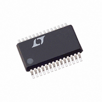
LTC1538CG-AUX Linear Technology, LTC1538CG-AUX Datasheet - Page 10

LTC1538CG-AUX
Manufacturer Part Number
LTC1538CG-AUX
Description
IC SW REG STP-DN SYNC DUAL28SSOP
Manufacturer
Linear Technology
Type
Step-Down (Buck)r
Specifications of LTC1538CG-AUX
Internal Switch(s)
No
Synchronous Rectifier
Yes
Number Of Outputs
2
Voltage - Output
1.19 ~ 9 V
Current - Output
50mA
Frequency - Switching
125kHz ~ 240kHz
Voltage - Input
3.5 ~ 36 V
Operating Temperature
0°C ~ 70°C
Mounting Type
Surface Mount
Package / Case
28-SSOP
Lead Free Status / RoHS Status
Contains lead / RoHS non-compliant
Power - Output
-
Available stocks
Company
Part Number
Manufacturer
Quantity
Price
Part Number:
LTC1538CG-AUX
Manufacturer:
LT/凌特
Quantity:
20 000
Part Number:
LTC1538CG-AUX#PBF
Manufacturer:
LINEAR/凌特
Quantity:
20 000
Company:
Part Number:
LTC1538CG-AUX-TR
Manufacturer:
FUJI
Quantity:
500
Part Number:
LTC1538CG-AUX-TR
Manufacturer:
LT/凌特
Quantity:
20 000
OPERATION
Main Control Loop
The LTC1538-AUX/LTC1539 use a constant frequency,
current mode step-down architecture. During normal op-
eration, the top MOSFET is turned on each cycle when the
oscillator sets the RS latch and turned off when the main
current comparator I1 resets the RS latch. The peak
inductor current at which I1 resets the RS latch is con-
trolled by the voltage on the I
output of each error amplifier (EA). The V
described in the Pin Functions, allows the EA to receive a
selectively attenuated output feedback voltage V
the SENSE
receive an output feedback voltage V
nal or external resistive dividers on the second controller.
When the load current increases, it causes a slight de-
crease in V
causes the I
inductor current matches the new load current. After the
large top MOSFET has turned off, the bottom MOSFET is
turned on until either the inductor current starts to reverse,
as indicated by current comparator I2, or the beginning of
the next cycle.
The top MOSFET drivers are biased from floating boot
strap capacitor C
each Off cycle. When V
V
turn on the top MOSFET continuously. The dropout detec-
tor counts the number of oscillator cycles that the top
MOSFET remains on and periodically forces a brief off
period to allow C
The main control loop is shut down by pulling the RUN/
SS1 (RUN/SS2) pin low. Releasing RUN/SS1 (RUN/SS2)
allows an internal 3 A current source to charge soft start
capacitor C
loop is enabled with the I
approximately 30% of its maximum value. As C
ues to charge, I
normal operation to resume. When both RUN/SS1 and
RUN/SS2 are low, all LTC1538-AUX/LTC1539 functions
are shut down except for the 5V standby regulator, internal
reference and a comparator. Refer to the LTC1438/LTC1439
for applications which do not require a 5V standby regulator.
LTC1538-AUX/LTC1539
10
OUT
, however, the loop may enter dropout and attempt to
–
FB
SS
TH1
1 pin while V
relative to the 1.19V reference, which in turn
. When C
(I
TH1
TH2
B
U
B
, which normally is recharged during
to recharge.
(I
) voltage to increase until the average
TH2
(Refer to Functional Diagram)
SS
IN
) is gradually released allowing
PROG2
decreases to a voltage close to
reaches 1.3V, the main control
TH1
TH1
(I
and V
TH2
(I
TH2
) voltage clamped at
FB2
OSENSE2
) pin, which is the
from either inter-
allow EA to
PROG1
SS
FB1
contin-
from
pin,
Comparator OV guards against transient overshoots
> 7.5% by turning off the top MOSFET and keeping it off
until the fault is removed.
Low Current Operation
Adaptive Power Mode allows the LTC1539 to automati-
cally change between two output stages sized for different
load currents. The TGL1 (TGL2) and BG1 (BG2) pins drive
large synchronous N-channel MOSFETs for operation at
high currents, while the TGS1 (TGS2) pin drives a much
smaller N-channel MOSFET used in conjunction with a
Schottky diode for operation at low currents. This allows
the loop to continue to operate at normal operating fre-
quency as the load current decreases without incurring the
large MOSFET gate charge losses. If the TGS1 (TGS2) pin
is left open, the loop defaults to Burst Mode operation in
which the large MOSFETs operate intermittently based on
load demand. Adaptive Power mode provides constant
frequency operation down to approximately 1% of rated
load current. This results in an order of magnitude reduc-
tion of load current before Burst Mode operation com-
mences. Without the small MOSFET (ie: no Adaptive
Power mode) the transition to Burst Mode operation is
approximately 10% of rated load current. The transition to
low current operation begins when comparator I2 detects
current reversal and turns off the bottom MOSFET. If the
voltage across R
I2 (approximately 20mV) for one full cycle, then on follow-
ing cycles the top drive is routed to the small MOSFET at
the TGS1 (TGS2) pin and the BG1 (BG2) pin is disabled.
This continues until an inductor current peak exceeds
20mV/R
either of which causes drive to be returned to the TGL1
(TGL2) pin on the next cycle.
Two conditions can force continuous synchronous opera-
tion, even when the load current would otherwise dictate
low current operation. One is when the common mode
voltage of the SENSE
(SENSE
SFB1 pin is below 1.19V. The latter condition is used to
assist in secondary winding regulation, as described in the
Applications Information section.
–
SENSE
2) pins are below 1.4V, and the other is when the
or the I
SENSE
does not exceed the hysteresis of
TH1
+
1 (SENSE
(I
TH2
) voltage exceeds 0.6V,
+
2) and SENSE
–
1


