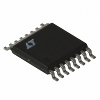
LT3434IFE#TR Linear Technology, LT3434IFE#TR Datasheet - Page 10

LT3434IFE#TR
Manufacturer Part Number
LT3434IFE#TR
Description
IC REG SW BUCK 3A 200KHZ 16TSSOP
Manufacturer
Linear Technology
Type
Step-Down (Buck)r
Datasheet
1.LT3434EFEPBF.pdf
(24 pages)
Specifications of LT3434IFE#TR
Internal Switch(s)
Yes
Synchronous Rectifier
No
Number Of Outputs
1
Voltage - Output
1.25 ~ 54 V
Current - Output
3A
Frequency - Switching
200kHz
Voltage - Input
3.3 ~ 60 V
Operating Temperature
-40°C ~ 125°C
Mounting Type
Surface Mount
Package / Case
16-TSSOP Exposed Pad, 16-eTSSOP, 16-HTSSOP
Lead Free Status / RoHS Status
Contains lead / RoHS non-compliant
Power - Output
-
Available stocks
Company
Part Number
Manufacturer
Quantity
Price
LT3434
APPLICATIO S I FOR ATIO
and Soft-Start Current graphs in Typical Performance
Characteristics).
Frequency foldback is done to control power dissipation in
both the IC and in the external diode and inductor during
short-circuit conditions. A shorted output requires the
switching regulator to operate at very low duty cycles. As
a result the average current through the diode and induc-
tor is equal to the short-circuit current limit of the switch
(typically 4.7A for the LT3434). Minimum switch on time
limitations would prevent the switcher from attaining a
sufficiently low duty cycle if switching frequency were
maintained at 200kHz, so frequency is reduced by about
4:1 when the FB pin voltage drops below 0.4V (see
Frequency Foldback graph). In addition, if the current in
the switch exceeds 1.5 times the current limitations speci-
fied by the V
LT3434 will skip the next switch cycle. As the feedback
voltage rises, the switching frequency increases to 200kHz
with 0.95V on the FB pin. During frequency foldback,
external syncronization is disabled to prevent interference
with foldback operation. Frequency foldback does not
affect operation during normal load conditions.
In addition to lowering switching frequency the soft-start
ramp rate is also affected by the feedback voltage. Large
capacitive loads or high input voltages can cause a high
input current surge during start-up. The soft-start func-
tion reduces input current surge by regulating switch
current via the V
rate (dV/dt) at the output. A capacitor (C1 in Figure 2) from
the C
dV/dt. When the feedback voltage is below 0.4V, the V
will rise, resulting in an increase in switch current and
output voltage. If the dV/dt of the output causes the current
through the C
reduced resulting in a constant dV/dt at the output. As the
feedback voltage increases I
increased dV/dt until the soft-start function is defeated
with 0.9V present at the FB pin. The soft-start function
does not affect operation during normal load conditions.
However, if a momentary short (brown out condition) is
present at the output which causes the FB voltage to drop
below 0.9V, the soft-start circuitry will become active.
10
SS
pin to the output determines the maximum output
C
SS
pin, due to minimum switch on time, the
C
capacitor to exceed I
pin to maintain a constant voltage ramp
U
U
CSS
increases, resulting in an
W
CSS
the V
C
U
voltage is
C
pin
INPUT CAPACITOR
Step-down regulators draw current from the input supply
in pulses. The rise and fall times of these pulses are very
fast. The input capacitor is required to reduce the voltage
ripple this causes at the input of LT3434 and force the
switching current into a tight local loop, thereby minimiz-
ing EMI. The RMS ripple current can be calculated from:
Ceramic capacitors are ideal for input bypassing. At 200kHz
switching frequency input capacitor values in the range of
4.7µF to 20µF are suitable for most applications. If opera-
tion is required close to the minimum input required by the
LT3434 a larger value may be required. This is to prevent
excessive ripple causing dips below the minimum operat-
ing voltage resulting in erratic operation.
Input voltage transients caused by input voltage steps or
by hot plugging the LT3434 to a pre-powered source such
as a wall adapter can exceed maximum V
sudden application of input voltage will cause a large
surge of current in the input leads that will store energy in
the parasitic inductance of the leads. This energy will
cause the input voltage to swing above the DC level of input
power source and it may exceed the maximum voltage
rating of the input capacitor and LT3434. All input voltage
transient sequences should be observed at the V
the LT3434 to ensure that absolute maximum voltage
ratings are not violated.
The easiest way to suppress input voltage transients is to
add a small aluminum electrolytic capacitor in parallel with
the low ESR input capacitor. The selected capacitor needs
to have the right amount of ESR to critically damp the
resonant circuit formed by the input lead inductance and
the input capacitor. The typical values of ESR will fall in the
range of 0.5Ω to 2Ω and capacitance will fall in the range
of 5µF to 50µF.
If tantalum capacitors are used, values in the 22µF to
470µF range are generally needed to minimize ESR and
meet ripple current and surge ratings. Care should be
I
RIPPLE RMS
(
)
=
I
OUT
V
IN
V
OUT
(
V
IN
–
V
OUT
)
IN
ratings. The
IN
pin of
3434fb


