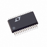
LTC1628IG-SYNC Linear Technology, LTC1628IG-SYNC Datasheet - Page 17

LTC1628IG-SYNC
Manufacturer Part Number
LTC1628IG-SYNC
Description
IC REG SW 2PH SYNC STPDWN 28SSOP
Manufacturer
Linear Technology
Type
Step-Down (Buck)r
Datasheet
1.LTC1628CG-SYNCPBF.pdf
(32 pages)
Specifications of LTC1628IG-SYNC
Internal Switch(s)
No
Synchronous Rectifier
Yes
Number Of Outputs
2
Voltage - Output
Adj to 0.8V
Current - Output
3A
Frequency - Switching
140kHz ~ 310kHz
Voltage - Input
3.5 ~ 30 V
Operating Temperature
-40°C ~ 85°C
Mounting Type
Surface Mount
Package / Case
28-SSOP
Lead Free Status / RoHS Status
Contains lead / RoHS non-compliant
Power - Output
-
Available stocks
Company
Part Number
Manufacturer
Quantity
Price
Company:
Part Number:
LTC1628IG-SYNC
Manufacturer:
INTEL
Quantity:
233
Part Number:
LTC1628IG-SYNC
Manufacturer:
LT/凌特
Quantity:
20 000
Part Number:
LTC1628IG-SYNC#PBF
Manufacturer:
LINEAR/凌特
Quantity:
20 000
APPLICATIO S I FOR ATIO
INTV
An internal P-channel low dropout regulator produces 5V
at the INTV
the drivers and internal circuitry within the LTC1628-
SYNC. The INTV
of 50mA and must be bypassed to ground with a mini-
mum of 4.7µF tantalum, 10µF special polymer, or low
ESR type electrolytic capacitor. A 1µF ceramic capacitor
placed directly adjacent to the INTV
is highly recommended. Good bypassing is necessary to
supply the high transient currents required by the MOSFET
gate drivers and to prevent interaction between channels.
Higher input voltage applications in which large MOSFETs
are being driven at high frequencies may cause the maxi-
mum junction temperature rating for the LTC1628-SYNC
to be exceeded. The system supply current is normally
dominated by the gate charge current. Additional external
loading of the INTV
needs to be taken into account for the power dissipation
calculations. The total INTV
either the 5V internal linear regulator or by the EXTV
input pin. When the voltage applied to the EXTV
less than 4.7V, all of the INTV
internal 5V linear regulator. Power dissipation for the IC in
this case is highest: (V
is lowered. The gate charge current is dependent on
operating frequency as discussed in the Efficiency Consid-
erations section. The junction temperature can be esti-
mated by using the equations given in Note 2 of the
Electrical Characteristics. For example, the LTC1628-SYNC
V
when not using the EXTV
Use of the EXTV
ture to:
Dissipation should be calculated to also include any added
current drawn from the internal 3.3V linear regulator. To
prevent maximum junction temperature from being ex-
ceeded, the input supply current must be checked operat-
ing in continuous mode at maximum V
IN
T
T
current is limited to less than 24mA from a 24V supply
J
J
CC
= 70°C + (24mA)(24V)(95°C/W) = 125°C
= 70°C + (24mA)(5V)(95°C/W) = 81°C
Regulator
CC
pin from the V
CC
CC
input pin reduces the junction tempera-
pin regulator can supply a peak current
U
CC
IN
and 3.3V linear regulators also
)(I
CC
U
INTVCC
CC
IN
pin as follows:
CC
supply pin. INTV
current can be supplied by
current is supplied by the
), and overall efficiency
W
CC
and PGND IC pins
IN
.
U
CC
CC
powers
pin is
CC
EXTV
The LTC1628-SYNC contains an internal P-channel MOS-
FET switch connected between the EXTV
pins. When the voltage applied to EXTV
4.7V, the internal regulator is turned off and the switch
closes, connecting the EXTV
thereby supplying internal power. The switch remains
closed as long as the voltage applied to EXTV
above 4.5V. This allows the MOSFET driver and control
power to be derived from the output during normal opera-
tion (4.7V < V
when the output is out of regulation (start-up, short-
circuit). If more current is required through the EXTV
switch than is specified, an external Schottky diode can be
added between the EXTV
greater than 7V to the EXTV
EXTV
Significant efficiency gains can be realized by powering
INTV
from the driver and control currents will be scaled by a
factor of (Duty Cycle)/(Efficiency). For 5V regulators this
supply means connecting the EXTV
However, for 3.3V and other lower voltage regulators,
additional circuitry is required to derive INTV
from the output.
The following list summarizes the four possible connec-
tions for EXTV
1. EXTV
TV
ing in an efficiency penalty of up to 10% at high input
voltages.
2. EXTV
connection for a 5V regulator and provides the highest
efficiency.
3. EXTV
supply is available in the 5V to 7V range, it may be used to
power EXTV
gate drive requirements.
4. EXTV
work. For 3.3V and other low voltage regulators, efficiency
gains can still be realized by connecting EXTV
CC
CC
CC
CC
to be powered from the internal 5V regulator result-
from the output, since the V
CC
CC
CC
CC
< V
Connection
Connected directly to V
Connected to an External supply. If an external
Left Open (or Grounded). This will cause IN-
Connected to an Output-Derived Boost Net-
IN
CC
.
OUT
CC:
providing it is compatible with the MOSFET
< 7V) and from the internal regulator
CC
LTC1628-SYNC
and INTV
CC
CC
pin to the INTV
OUT
CC
pin and ensure that
CC
IN
pin directly to V
. This is the normal
pins. Do not apply
current resulting
CC
CC
rises above
and INTV
CC
CC
CC
remains
17
1628syncfa
CC
power
to an
OUT
pin
CC
CC
.


