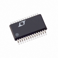
LTC1628IG Linear Technology, LTC1628IG Datasheet - Page 18

LTC1628IG
Manufacturer Part Number
LTC1628IG
Description
IC SW REG STEP-DOWN 28-SSOP
Manufacturer
Linear Technology
Type
Step-Down (Buck)r
Datasheet
1.LTC1628CGPBF.pdf
(32 pages)
Specifications of LTC1628IG
Internal Switch(s)
No
Synchronous Rectifier
Yes
Number Of Outputs
2
Voltage - Output
Adj to 0.8V
Current - Output
3A
Frequency - Switching
220kHz
Voltage - Input
3.5 ~ 30 V
Operating Temperature
-40°C ~ 85°C
Mounting Type
Surface Mount
Package / Case
28-SSOP
Lead Free Status / RoHS Status
Contains lead / RoHS non-compliant
Power - Output
-
Other names
Q1109473
Available stocks
Company
Part Number
Manufacturer
Quantity
Price
Company:
Part Number:
LTC1628IG
Manufacturer:
Linear
Quantity:
470
Part Number:
LTC1628IG
Manufacturer:
LT
Quantity:
20 000
Part Number:
LTC1628IG#PBF
Manufacturer:
LINEAR/凌特
Quantity:
20 000
Part Number:
LTC1628IG#TRPBF
Manufacturer:
LT
Quantity:
20 000
Part Number:
LTC1628IG-PG#PBF
Manufacturer:
LINEAR/凌特
Quantity:
20 000
Company:
Part Number:
LTC1628IG-SYNC
Manufacturer:
INTEL
Quantity:
233
Part Number:
LTC1628IG-SYNC
Manufacturer:
LT/凌特
Quantity:
20 000
Company:
Part Number:
LTC1628IGTR
Manufacturer:
HYN
Quantity:
3 229
APPLICATIO S I FOR ATIO
LTC1628/LTC1628-PG
derived from the output during normal operation (4.7V <
V
is out of regulation (start-up, short-circuit). If more cur-
rent is required through the EXTV
fied, an external Schottky diode can be added between the
EXTV
the EXTV
Significant efficiency gains can be realized by powering
INTV
from the driver and control currents will be scaled by a
factor of (Duty Cycle)/(Efficiency). For 5V regulators this
supply means connecting the EXTV
However, for 3.3V and other lower voltage regulators,
additional circuitry is required to derive INTV
from the output.
The following list summarizes the four possible connec-
tions for EXTV
1. EXTV
to be powered from the internal 5V regulator resulting in
an efficiency penalty of up to 10% at high input voltages.
2. EXTV
connection for a 5V regulator and provides the highest
efficiency.
3. EXTV
supply is available in the 5V to 7V range, it may be used to
power EXTV
gate drive requirements.
18
OUT
R6
R5
Figure 6a. Secondary Output Loop & EXTV
CC
< 7V) and from the internal regulator when the output
CC
OPTIONAL EXTV
CONNECTION
5V < V
EXTV
FCB
SGND
from the output, since the V
CC
CC
CC
and INTV
CC
Left Open (or Grounded). This will cause INTV
Connected directly to V
Connected to an External supply. If an external
CC
SEC
LTC1628
pin and ensure that EXTV
CC
< 7V
CC:
providing it is compatible with the MOSFET
PGND
CC
CC
BG1
TG1
SW
V
U
IN
pins. Do not apply greater than 7V to
N-CH
N-CH
U
V
IN
+
CC
OUT
C
CC
W
IN
switch than is speci-
1:N
T1
IN
pin directly to V
CC
. This is the normal
current resulting
< V
CC
Connection
R
IN
SENSE
V
.
SEC
U
CC
+
+
power
1628 F06a
1 F
C
OUT
V
OUT
OUT
CC
.
4. EXTV
work. For 3.3V and other low voltage regulators, efficiency
gains can still be realized by connecting EXTV
output-derived voltage that has been boosted to greater
than 4.7V. This can be done with either the inductive boost
winding as shown in Figure 6a or the capacitive charge
pump shown in Figure 6b. The charge pump has the
advantage of simple magnetics.
Topside MOSFET Driver Supply (C
External bootstrap capacitors C
pins supply the gate drive voltages for the topside MOSFETs.
Capacitor C
external diode D
When one of the topside MOSFETs is to be turned on, the
driver places the C
desired MOSFET. This enhances the MOSFET and turns on
the topside switch. The switch node voltage, SW, rises to
V
on, the boost voltage is above the input supply: V
V
to be 100 times that of the total input capacitance of the
topside MOSFET(s). The reverse breakdown of the exter-
nal Schottky diode must be greater than V
adjusting the gate drive level, the final arbiter is the total
input current for the regulator. If a change is made and the
input current decreases, then the efficiency has improved.
If there is no change in input current, then there is no
change in efficiency.
IN
IN
and the BOOST pin follows. With the topside MOSFET
+ V
EXTV
INTVCC
CC
Figure 6b. Capacitive Charge Pump for EXTV
CC
LTC1628
Connected to an Output-Derived Boost Net-
B
in the functional diagram is charged though
. The value of the boost capacitor C
PGND
BG1
TG1
SW
V
IN
B
from INTV
B
C
IN
voltage across the gate-source of the
N-CH
N-CH
+
V
IN
CC
BAT85
B
when the SW pin is low.
connected to the BOOST
L1
B
, D
VN2222LL
0.22 F
B
R
)
SENSE
IN(MAX)
+
+
CC
1628 F06b
CC
BAT85
1 F
BAT85
C
B
BOOST
V
. When
OUT
OUT
needs
to an
1628fb
=


