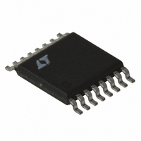
LT1765EFE-3.3 Linear Technology, LT1765EFE-3.3 Datasheet - Page 14

LT1765EFE-3.3
Manufacturer Part Number
LT1765EFE-3.3
Description
IC REG SW STEPDOWN 3A 16-TSSOP
Manufacturer
Linear Technology
Type
Step-Down (Buck)r
Datasheet
1.LT1765ES8PBF.pdf
(20 pages)
Specifications of LT1765EFE-3.3
Internal Switch(s)
Yes
Synchronous Rectifier
No
Number Of Outputs
1
Voltage - Output
3.3V
Current - Output
3A
Frequency - Switching
1.25MHz
Voltage - Input
3 ~ 25 V
Operating Temperature
-40°C ~ 125°C
Mounting Type
Surface Mount
Package / Case
16-TSSOP Exposed Pad, 16-eTSSOP, 16-HTSSOP
Lead Free Status / RoHS Status
Contains lead / RoHS non-compliant
Power - Output
-
Available stocks
Company
Part Number
Manufacturer
Quantity
Price
Part Number:
LT1765EFE-3.3
Manufacturer:
LINEAR/凌特
Quantity:
20 000
Company:
Part Number:
LT1765EFE-3.3#PBF
Manufacturer:
LT
Quantity:
7 000
Company:
Part Number:
LT1765EFE-3.3#TRPBF
Manufacturer:
LT
Quantity:
7 000
Part Number:
LT1765EFE-3.3#TRPBF
Manufacturer:
LINEAR/凌特
Quantity:
20 000
APPLICATIONS INFORMATION
APPLICATIONS INFORMATION
LT1765/LT1765-1.8/LT1765-2.5/
LT1765-3.3/LT1765-5
Figure 8 shows the overall loop response with a 330pF VC
capacitor and a typical 100μF tantalum output capacitor.
The response is set by the following terms:
Error amplifi er:
DC gain set by g
Pole set by C
Unity-gain set by C
410kHz.
Power stage:
DC gain set by g
Pole set by C
Unity-gain set by C
8kHz.
Tantalum output capacitor:
Zero set by C
The zero produced by the ESR of the tantalum output capaci-
tor is very useful in maintaining stability. Ceramic output
capacitors do not have a zero due to very low ESR, but are
dominated by their ESL. They form a notch in the 1MHz to
10MHz range. Without this zero, the V
dominant. A typical value of 2.2nF will achieve this.
If better transient response is required, a zero can be
added to the loop using a resistor (R
compensation capacitor. As the value of R
transient response will generally improve, but two effects
limit its value. First, the combination of output capacitor
ESR and a large R
14
–20
–40
80
60
40
20
0
OUT
10
F
OUT
Figure 8. Overall Loop Response
and R
and C
C
m
and R
may stop loop gain rolling off altogether.
100
F
m
OUT
and R
and g
L
ESR
and R
FREQUENCY (Hz)
= (2π • 500k • 330p)
L
and g
1k
= (2π • 100μ • 0.1)
= (2π • 100μ • 10)
L
m
(assume 5Ω) = 5 • 5 = 25.
= (2π • 330p • 850μ
L
V
C
C
R
I
m
LOAD
OUT
OUT
C
C
10k
/C
= 850μ • 500k = 425.
= 330pF
= (2π • 100μ • 5
F
= 5V
= 100μF, 0.1Ω
= 0
= 1A
100k
C
C
) in series with the
PHASE
GAIN
pole must be made
1765 F08
C
1M
–1
is increased,
180
150
120
90
60
30
0
–1
–1
= 15.9kHz.
= 965Hz.
= 159Hz.
–1
–1
)
)
–1
–1
=
=
Second, if the loop gain is not rolled suffi ciently at the
switching frequency, output ripple will perturb the V
enough to cause unstable duty cycle switching similar
to subharmonic oscillation. This may not be apparent
at the output. Small signal analysis will not show this
since a continuous time system is assumed. If needed,
an additional capacitor (C
form a pole at typically one fi fth the switching frequency
(If R
When checking loop stability, the circuit should be operated
over the application’s full voltage, current and temperature
range. Any transient loads should be applied and the output
voltage monitored for a well-damped behavior.
CONVERTER WITH BACKUP OUTPUT REGULATOR
In systems with a primary and backup supply, for example,
a battery powered device with a wall adapter input, the
output of the LT1765 can be held up by the backup supply
with its input disconnected. In this condition, the SW pin
will source current into the V
at ground, only the shutdown current of 6μA will be pulled
via the SW pin from the second supply. With the SHDN pin
fl oating, the LT1765 will consume its quiescent operating
current of 1mA. The V
any other components connected to the input line. If this
load is greater than 10mA or the input could be shorted to
ground, a series Schottky diode must be added, as shown
in Figure 9. With these safeguards, the output can be held
at voltages up to the V
BUCK CONVERTER WITH ADJUSTABLE SOFT-START
Large capacitive loads or high input voltages can cause
high input currents at start-up. Figure 10 shows a circuit
that limits the dv/dt of the output at start-up, controlling
the capacitor charge rate. The buck converter is a typical
confi guration with the addition of R3, R4, C
the output starts to rise, Q1 turns on, regulating switch
current via the V
output. Output rise time is controlled by the current through
C
regulation, Q1 turns off and the circuit operates normally.
R3 is transient protection for the base of Q1.
SS
C
defi ned by R4 and Q1’s V
= ~ 5k, C
F
C
= ~ 100pF)
pin to maintain a constant dv/dt at the
IN
IN
absolute maximum rating.
F
pin will also source current to
) can be added to the V
IN
pin. If the SHDN pin is held
BE
. Once the output is in
SS
and Q1. As
C
pin to
C
1765fd
pin


