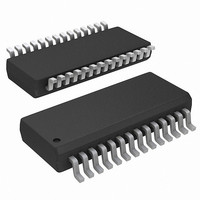
LTC3788IGN-1#PBF Linear Technology, LTC3788IGN-1#PBF Datasheet - Page 9

LTC3788IGN-1#PBF
Manufacturer Part Number
LTC3788IGN-1#PBF
Description
IC CTLR BOOST 2PH DUAL 28SSOP
Manufacturer
Linear Technology
Type
Step-Up (Boost)r
Datasheet
1.LTC3788EGN-1PBF.pdf
(30 pages)
Specifications of LTC3788IGN-1#PBF
Internal Switch(s)
No
Synchronous Rectifier
Yes
Number Of Outputs
2
Voltage - Output
Adj to 60V
Current - Output
25A
Frequency - Switching
105kHz ~ 760kHz
Voltage - Input
4.5 ~ 38 V
Operating Temperature
-40°C ~ 125°C
Mounting Type
Surface Mount
Package / Case
28-SSOP
Lead Free Status / RoHS Status
Lead free / RoHS Compliant
Power - Output
-
Available stocks
Company
Part Number
Manufacturer
Quantity
Price
PIN FUNCTIONS
SENSE1
Sense Comparator Input. The (–) input to the current
comparator is normally connected to the negative terminal
of a current sense resistor connected in series with the
inductor.The common mode voltage range on these pins
is 2.5V to 38V (40V abs max).
FREQ (Pin 5): The frequency control pin for the internal
VCO. Connecting the pin to GND forces the VCO to a fi xed
low frequency of 350kHz. Connecting the pin to INTV
forces the VCO to a fi xed high frequency of 535kHz. The
frequency can be programmed from 50kHz to 900kHz
by connecting a resistor from the FREQ pin to GND. The
resistor and an internal 20μA source current create a volt-
age used by the internal oscillator to set the frequency.
Alternatively, this pin can be driven with a DC voltage to
vary the frequency of the internal oscillator.
PLLIN/MODE (Pin 6): External Synchronization Input
to Phase Detector and Forced Continuous Mode Input.
When an external clock is applied to this pin, it will force
the controller into forced continuous mode of operation
and the phase-locked loop will force the rising BG1 signal
to be synchronized with the rising edge of the external
clock. When not synchronizing to an external clock, this
input, which acts on both controllers, determines how the
LTC3788-1 operates at light loads. Pulling this pin to ground
selects Burst Mode operation. An internal 100k resistor to
ground also invokes Burst Mode operation when the pin is
fl oated. Tying this pin to INTV
current operation. Tying this pin to a voltage greater than
1.2V and less than INTV
operation. This can be done by adding a 100k resistor
between the PLLIN/MODE pin and INTV
SGND (Pin 7): Signal Ground. All small-signal components
and compensation components should connect to this
ground, which in turn connects to PGND at a single point.
RUN1, RUN2 (Pin 8, Pin 9): Run Control Input. An external
resistor divider connects to V
converter operation with a threshold of 1.28V. Once running,
a 4.5μA current is sourced from the RUN pin allowing the
user to program hysteresis using the resistor values.
–
, SENSE2
–
(Pin 4, Pin 10): Negative Current
CC
– 1.3V selects pulse-skipping
CC
IN
forces continuous inductor
and sets the thresholds for
CC
.
CC
INTV
supply for control circuits and gate drives. Decouple this
pin to GND with a minimum 4.7μF low ESR tantalum or
ceramic capacitor.
EXTV
higher than 4.8V an internal switch bypasses the inter-
nal regulator and supply power to INTV
EXTV
PGND (Pin 21): Driver Power Ground. Connects to the
sources of bottom (main) N-channel MOSFETs and the
(–) terminal(s) of C
VBIAS (Pin 22): Main Supply Pin. It is normally tied to the
input supply V
bypass capacitor should be tied between this pin and the
signal ground pin.The operating voltage range on this pin
is 4.5V to 38V (40V abs max).
BG1, BG2 (Pin 23, Pin 18): Bottom Gate. Connect to the
gate of the main NMOS.
BOOST1, BOOST2 (Pin 24, Pin 17): Floating power supply
for the synchronous NMOS. Bypass to SW with a capacitor
and supply with a Schottky diode connected to INTV
TG1, TG2 (Pin 25, Pin 16): Top Gate. Connect to the gate
of the synchronous NMOS.
SW1, SW2 (Pin 26, Pin 15): Switch Node. Connect to the
source of the synchronous NMOS, the drain of the main
NMOS and the inductor.
PGOOD1 (Pin 27): Power Good Indicator for Channel 1.
Open-drain logic output that is pulled to ground when
the output voltage is more than ±10% away from the
regulated output voltage. To avoid false trips the output
voltage must be outside the range for 25μs before this
output is activated.
SS1, SS2 (Pin 28, Pin 14): Output Soft-Start Input. A
capacitor to ground at this pin sets the ramp rate of the
output voltage during start-up.
CC
CC
CC
.
(Pin 19): Output of Internal 5.4V LDO. Power
(Pin 20): External Power Input. When this pin is
IN
or to the output of the boost converter. A
IN
and C
OUT
.
LTC3788-1
CC
directly from
37881fa
CC
9
.


