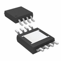
LT3663EMS8E-5#PBF Linear Technology, LT3663EMS8E-5#PBF Datasheet - Page 8

LT3663EMS8E-5#PBF
Manufacturer Part Number
LT3663EMS8E-5#PBF
Description
IC BUCK 5V 1.2A 8MSOP
Manufacturer
Linear Technology
Type
Step-Down (Buck)r
Datasheet
1.LT3663EDCBTRMPBF.pdf
(16 pages)
Specifications of LT3663EMS8E-5#PBF
Internal Switch(s)
Yes
Synchronous Rectifier
No
Number Of Outputs
1
Voltage - Output
5V
Current - Output
1.2A
Frequency - Switching
1MHz
Voltage - Input
7.5 ~ 36 V
Operating Temperature
-40°C ~ 125°C
Mounting Type
Surface Mount
Package / Case
8-MSOP Exposed Pad, 8-HMSOP, 8-eMSOP
Primary Input Voltage
36V
No. Of Outputs
1
Output Voltage
5V
Output Current
1.2A
No. Of Pins
8
Operating Temperature Range
-40°C To +125°C
Msl
MSL 1 - Unlimited
Switching Frequency Max
1.65MHz
Rohs Compliant
Yes
Lead Free Status / RoHS Status
Lead free / RoHS Compliant
Power - Output
-
Available stocks
Company
Part Number
Manufacturer
Quantity
Price
LT3663
FB Resistor Network
The output voltage of the LT3663 is programmed with a
resistor divider. Choose the 1% resistors according to:
Reference designators refer to the Block Diagram.
The resistor divider is internal on the fi xed output voltage
versions, LT3663-X.
Minimum Duty Cycle
As the input voltage increases the duty cycle decreases. At
some point, the minimum duty cycle of the IC is reached
and pulse skipping begins. The output voltage continues to
regulate but the output voltage ripple increases. The input
voltage at which this occurs is calculated as follows:
Where V
D1, and V
Q1. LT3663 DC
For V
occurs at about 24.5V.
Figure 1 illustrates switching waveforms in normal mode
for a 3.3V output application with V
APPLICATIONS INFORMATION
8
R1 = R2 (V
V
AC-COUPLED
IN
F
200mV/DIV
= 0.4V, V
=
20V/DIV
1A/DIV
F
(
V
V
SW
V
is the forward voltage drop of the catch diode,
OUT
SW
OUT
I
DC
L
is the voltage drop on the internal switch,
OUT
MIN
MIN
SW
+
Figure 1. Normal Operation
/0.8 – 1)
V
F
= 0.3V, and V
is typically 0.12.
)
–
V
F
+
2.5μs/DIV
V
SW
OUT
= 3.3V pulse skipping
IN
= 20V.
3663 F01
Figure 2. illustrates switching waveforms in pulse skip
mode a 3.3V output application with V
Inductor Selection
A good fi rst choice for the inductor value is:
where V
and L is in μH. With this value there is no sub-harmonic
oscillation for applications with 50% or greater duty
cycle. The inductor’s RMS current rating must be greater
than the maximum load current. Size the inductor so the
saturation current rating is about 30% higher than the
maximum load current. The output current limit circuit
tightly controls the maximum average inductor current,
therefore the inductor RMS current rating does not have
to be overrated to handle short circuit or overload condi-
tions. For high effi ciency, keep the series resistance (DCR)
less than 0.1Ω. A higher value inductor is larger in size
and slows transient response but reduces output voltage
ripple. A lower value inductor has higher ripple currents
but is physically smaller or, for the same size, it has lower
DCR typically resulting in higher effi ciency.
L = V
AC-COUPLED
200mV/DIV
20V/DIV
1A/DIV
OUT
D
V
V
OUT
is the voltage drop of the catch diode (~0.4V)
SW
I
L
+ V
D
Figure 2. Pulse-Skip Mode
(μH)
2.5μs/DIV
IN
= 30V.
3663 F02
3663fb


