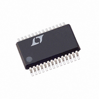
LTC3728LEGN-1#PBF Linear Technology, LTC3728LEGN-1#PBF Datasheet - Page 10

LTC3728LEGN-1#PBF
Manufacturer Part Number
LTC3728LEGN-1#PBF
Description
IC REG SYNC DUAL 28-SSOP
Manufacturer
Linear Technology
Series
PolyPhase®r
Type
Step-Down (Buck)r
Datasheet
1.LTC3728LEGN-1PBF.pdf
(32 pages)
Specifications of LTC3728LEGN-1#PBF
Internal Switch(s)
No
Synchronous Rectifier
Yes
Number Of Outputs
2
Voltage - Output
0.8 ~ 7 V
Current - Output
3A
Frequency - Switching
250kHz ~ 550kHz
Voltage - Input
4.5 ~ 28 V
Operating Temperature
-40°C ~ 85°C
Mounting Type
Surface Mount
Package / Case
28-SSOP
Lead Free Status / RoHS Status
Lead free / RoHS Compliant
Power - Output
-
Available stocks
Company
Part Number
Manufacturer
Quantity
Price
OPERATION
LTC3728L-1
Main Control Loop
The LTC3728L-1 is a constant frequency, current mode
step-down controller with two channels operating 180
degrees out of phase. During normal operation, each top
MOSFET is turned on when the clock for that channel sets
the RS latch, and turned off when the main current com-
parator, I
at which I
on the I
EA. The V
which is compared to the internal reference voltage by the
EA. When the load current increases, it causes a slight
decrease in V
in turn causes the I
inductor current matches the new load current. After the
top MOSFET has turned off, the bottom MOSFET is turned
on until either the inductor current starts to reverse, as
indicated by current comparator I
the next cycle.
The top MOSFET drivers are biased from fl oating bootstrap
capacitor C
cycle through an external diode when the top MOSFET
turns off. As V
loop may enter dropout and attempt to turn on the top
MOSFET continuously. The dropout detector detects this
and forces the top MOSFET off for about 400ns every tenth
cycle to allow C
The main control loop is shut down by pulling the RUN/SS
pin low. Releasing RUN/SS allows an internal 1.2μA cur-
rent source to charge soft-start capacitor C
reaches 1.5V, the main control loop is enabled with the I
voltage clamped at approximately 30% of its maximum
value. As C
gradually released allowing normal, full-current operation.
When both RUN/SS1 and RUN/SS2 are low, all controller
functions are shut down, including the 5V regulator.
Low Current Operation
The FCB pin is a multifunction pin providing two func-
tions: 1) to provide regulation for a secondary winding
10
TH
1
OSENSE
1
, resets the RS latch. The peak inductor current
pin, which is the output of each error amplifi er
resets the RS latch is controlled by the voltage
B
SS
, which normally is recharged during each off
OSENSE
IN
continues to charge, the I
B
decreases to a voltage close to V
pin receives the voltage feedback signal,
to recharge.
TH
relative to the 0.8V reference, which
voltage to increase until the average
(Refer to Functional Diagram)
2
, or the beginning of
TH
SS
pin voltage is
. When C
OUT
, the
SS
TH
by temporarily forcing continuous PWM operation on
both controllers; and 2) to select between two modes
of low current operation. When the FCB pin voltage is
below 0.8V, the controller forces continuous PWM cur-
rent mode operation. In this mode, the top and bottom
MOSFETs are alternately turned on to maintain the output
voltage independent of direction of inductor current.
When the FCB pin is below V
than 0.8V, the controller enters Burst Mode operation.
Burst Mode operation sets a minimum output current
level before inhibiting the top switch and turns off the
synchronous MOSFET(s) when the inductor current goes
negative. This combination of requirements will, at low
currents, force the I
will temporarily inhibit turn-on of both output MOSFETs
until the output voltage drops. There is 60mV of hyster-
esis in the burst comparator B tied to the I
hysteresis produces output signals to the MOSFETs that
turn them on for several cycles, followed by a variable
“sleep” interval depending upon the load current. The
resultant output voltage ripple is held to a very small
value by having the hysteretic comparator after the error
amplifi er gain block.
Frequency Synchronization
The phase-locked loop allows the internal oscillator to
be synchronized to an external source via the PLLIN pin.
The output of the phase detector at the PLLFLTR pin is
also the DC frequency control input of the oscillator that
operates over a 260kHz to 550kHz range corresponding
to a DC voltage input from 0V to 2.4V. When locked, the
PLL aligns the turn on of the top MOSFET to the rising
edge of the synchronizing signal. When PLLIN is left
open, the PLLFLTR pin goes low, forcing the oscillator to
minimum frequency.
Constant Frequency Operation
When the FCB pin is tied to INTV
tion is disabled and the forced minimum output current
requirement is removed. This provides constant frequency,
discontinuous current (preventing reverse inductor cur-
rent) operation over the widest possible output current
range. This constant frequency operation is not as effi cient
TH
pin below a voltage threshold that
INTVCC
CC
, Burst Mode opera-
– 2V but greater
TH
pin. This
3728l1fc


