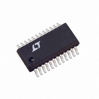
LTC3736EGN-1#TR Linear Technology, LTC3736EGN-1#TR Datasheet - Page 22

LTC3736EGN-1#TR
Manufacturer Part Number
LTC3736EGN-1#TR
Description
IC CTRLR SW SYNC DUAL 2PH 24SSOP
Manufacturer
Linear Technology
Series
PolyPhase®r
Type
Step-Down (Buck)r
Datasheet
1.LTC3736EGN-1.pdf
(28 pages)
Specifications of LTC3736EGN-1#TR
Internal Switch(s)
No
Synchronous Rectifier
Yes
Number Of Outputs
2
Voltage - Output
0.6 ~ 9.8 V
Current - Output
1A
Frequency - Switching
450kHz ~ 580kHz
Voltage - Input
2.75 ~ 9.8 V
Operating Temperature
-40°C ~ 85°C
Mounting Type
Surface Mount
Package / Case
24-SSOP
Lead Free Status / RoHS Status
Contains lead / RoHS non-compliant
Power - Output
-
APPLICATIO S I FOR ATIO
LTC3736-1
at the FETs. It is better to have two separate, smaller valued
input capacitors (e.g., two 10µF—one for each channel)
than it is to have a single larger valued capacitor (e.g.,
22µF) that the channels share with a common connection.
2) The signal and power grounds should be kept separate.
The signal ground consists of the feedback resistor divid-
ers, I
The power grounds consist of the (–) terminal of the input
and output capacitors and the source of the N-channel
MOSFET. Each channel should have its own power ground
for its power loop (as described in (1) above). The power
grounds for the two channels should connect together at
a common point. It is most important to keep the ground
paths with high switching currents away from each other.
22
TH
compensation networks and the SGND pin.
R
U
IN
V
IN
C
IN
BOLD LINES INDICATE
HIGH, SWITCHING
CURRENT LINES.
KEEP LINES TO A
MINIMUM LENGTH
U
+
W
Figure 12. Branch Current Waveforms
MP1
MP2
U
MN1
MN2
The PGND pins on the LTC3736-1 IC should be shorted
together and connected to the common power ground
connection (away from the switching currents).
3) Put the feedback resistors close to the V
trace connecting the top feedback resistor (R
output capacitor should be a Kelvin trace. The I
sation components should also be very close to the
LTC3736-1.
4) The current sense traces (SENSE
Kelvin connections right at the P-channel MOSFET source
and drain.
5) Keep the switch nodes (SW1, SW2) and the gate driver
nodes (TG1, TG2, BG1, BG2) away from the small-signal
components, especially the opposite channels feedback
resistors, I
sense pins (SENSE
L1
L2
C
C
TH
OUT1
OUT2
compensation components and the current
V
V
+
+
OUT1
OUT2
+
and SW).
37361 F12
R
R
+
L1
L2
and SW) should be
FB
TH
pins. The
B
compen-
) to the
37361f


