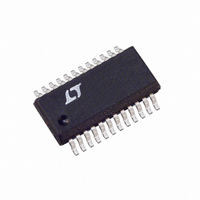
LTC1702ACGN#TR Linear Technology, LTC1702ACGN#TR Datasheet - Page 21

LTC1702ACGN#TR
Manufacturer Part Number
LTC1702ACGN#TR
Description
IC SW REG SYNC 550KHZ DUAL24SSOP
Manufacturer
Linear Technology
Series
PolyPhase®r
Type
Step-Down (Buck)r
Datasheet
1.LTC1702ACGNPBF.pdf
(36 pages)
Specifications of LTC1702ACGN#TR
Internal Switch(s)
No
Synchronous Rectifier
No
Number Of Outputs
2
Voltage - Output
0.8 ~ 7 V
Current - Output
1A, 25A
Frequency - Switching
550kHz
Voltage - Input
3 ~ 7 V
Operating Temperature
0°C ~ 70°C
Mounting Type
Surface Mount
Package / Case
24-SSOP
Lead Free Status / RoHS Status
Contains lead / RoHS non-compliant
Power - Output
-
Other names
LTC1702ACGNTR
Available stocks
Company
Part Number
Manufacturer
Quantity
Price
APPLICATIONS
output, with the attendant 180° phase shift. This roll-off is
what filters the PWM waveform, resulting in the desired
DC output voltage, but the phase shift complicates the
loop compensation if the gain is still higher than unity at
the pole frequency. Eventually (usually well above the LC
pole frequency), the reactance of the output capacitor will
approach its ESR, and the roll-off due to the capacitor will
stop, leaving 6dB/octave and 90° of phase shift (Figure 8).
GAIN
(dB)
GAIN
(dB)
Figure 9a. Type 1 Amplifier Schematic Diagram
Figure 8. Transfer Function of Buck Modulator
A
Figure 9b. Type 1 Amplifier Transfer Function
0
V
0
IN
GAIN
PHASE
R1
PHASE
U
R
B
GAIN
V
–12dB/OCT
INFORMATION
REF
U
+
–
C1
–6dB/OCT
W
–6dB/OCT
1702A F09a
OUT
1702A F09b
1702A F08
PHASE
0
–90
–180
(DEG)
0
–90
–180
–270
PHASE
(DEG)
U
So far, the AC response of the loop is pretty well out of the
user’s control. The modulator is a fundamental piece of the
LTC1702A design, and the external L and C are usually
chosen based on the regulation and load current require-
ments without considering the AC loop response. The
feedback amplifier, on the other hand, gives us a handle
with which to adjust the AC response. The goal is to have
180° phase shift at DC (so the loop regulates) and some-
thing less than 360° phase shift at the point that the loop
gain falls to 0dB. The simplest strategy is to set up the
feedback amplifier as an inverting integrator, with the 0dB
frequency lower than the LC pole (Figure 9). This “type 1”
configuration is stable but transient response will be less
than exceptional if the LC pole is at a low frequency.
Figure 10 shows an improved “type 2” circuit that uses an
additional pole-zero pair to temporarily remove 90° of
phase shift. This allows the loop to remain stable with 90°
more phase shift in the LC section, provided the loop
reaches 0dB gain near the center of the phase “bump.”
GAIN
(dB)
Figure 10a. Type 2 Amplifier Schematic Diagram
Figure 10b. Type 2 Amplifier Transfer Function
0
IN
GAIN
PHASE
R1
–6dB/OCT
R
B
V
REF
R2
+
–
C2
–6dB/OCT
C1
LTC1702A
1702A F10a
OUT
PHASE
0
–90
–180
–270
(DEG)
1702A F10b
21
1702afa


