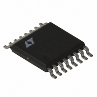
LT1977IFE Linear Technology, LT1977IFE Datasheet - Page 17

LT1977IFE
Manufacturer Part Number
LT1977IFE
Description
IC REG SW 1.5A HV STPDWN 16TSSOP
Manufacturer
Linear Technology
Type
Step-Down (Buck)r
Datasheet
1.LT1977EFEPBF.pdf
(24 pages)
Specifications of LT1977IFE
Internal Switch(s)
Yes
Synchronous Rectifier
No
Number Of Outputs
1
Voltage - Output
1.2 ~ 54 V
Current - Output
1.5A
Frequency - Switching
500kHz
Voltage - Input
3.3 ~ 60 V
Operating Temperature
-40°C ~ 125°C
Mounting Type
Surface Mount
Package / Case
16-TSSOP Exposed Pad, 16-eTSSOP, 16-HTSSOP
Lead Free Status / RoHS Status
Contains lead / RoHS non-compliant
Power - Output
-
Available stocks
Company
Part Number
Manufacturer
Quantity
Price
Company:
Part Number:
LT1977IFE#PBF
Manufacturer:
LT
Quantity:
2 500
Part Number:
LT1977IFE#PBF
Manufacturer:
LINEAR/凌特
Quantity:
20 000
APPLICATIO S I FOR ATIO
must weigh the importance of each specification in choos-
ing the best diode for the application.
The use of so-called “ultrafast” recovery diodes is gener-
ally not recommended. When operating in continuous
mode, the reverse recovery time exhibited by “ultrafast”
diodes will result in a slingshot type effect. The power
internal switch will ramp up V
attempt to get it to recover. Then, when the diode has
finally turned off, some tens of nanoseconds later, the V
node voltage ramps up at an extremely high dV/dt, per-
haps 5V to even 10V/ns! With real world lead inductances
the V
result in poor RFI behavior and, if the overshoot is severe
enough, damage the IC itself.
BOOST PIN
For most applications the boost components are a 0.1µF
capacitor and a MMSD914 diode. The anode is typically
connected to the regulated output voltage to generate a
voltage approximately V
stage (Figure 7a). However, the output stage discharges
the boost capacitor during the on time of the switch. The
output driver requires at least 2.5V of headroom through-
out this period to keep the switch fully saturated. If the
output voltage is less than 3.3V it is recommended that an
alternate boost supply is used. The boost diode can be
connected to the input (Figure 7b) but care must be taken
to prevent the boost voltage (V
exceeding the BOOST pin absolute maximum rating. The
additional voltage across the switch driver also increases
power loss and reduces efficiency. If available, an inde-
pendent supply can be used to generate the required
BOOST voltage (Figure 7c). Tying BOOST to V
independent supply may reduce efficiency but it will re-
duce the minimum V
loads. If the generated BOOST voltage dissipates too
much power at maximum load, the BOOST voltage the
LT1977 sees can be reduced by placing a Zener diode in
series with the BOOST diode (Figure 7a option).
A 0.1µF boost capacitor is recommended for most appli-
cations. Almost any type of film or ceramic capacitor is
suitable but the ESR should be <1Ω to ensure it can be fully
recharged during the off time of the switch. The capacitor
SW
node can easily overshoot the V
U
IN
OUT
required to start-up with light
U
above V
IN
current into the diode in an
BOOST
W
IN
to drive the output
= V
IN
rail. This can
IN
U
• 2) from
IN
or an
SW
value is derived from worst-case conditions of 1800ns on
time, 40mA boost current and 0.7V discharge ripple. The
boost capacitor value could be reduced under less de-
manding conditions but this will not improve circuit opera-
tion or efficiency. Under low input voltage and low load
conditions a higher value capacitor will reduce discharge
ripple and improve start-up operation.
SHUTDOWN FUNCTION AND UNDERVOLTAGE
LOCKOUT
The SHDN pin on the LT1977 controls the operation of the
IC. When the voltage on the SHDN pin is below the 1.2V
shutdown threshold the LT1977 is placed in a “zero”
supply current state. Driving the SHDN pin above the
shutdown threshold enables normal operation. The SHDN
pin has an internal sink current of 3µA.
V
V
V
IN
IN
IN
Figure 7. BOOST Pin Configurations
V
V
BOOST(MAX)
BOOST(MAX)
V
V
V
V
BOOST
BOOST
BOOST
BOOST(MAX)
V
GND
V
GND
V
GND
IN
IN
IN
LT1977
LT1977
LT1977
– V
– V
– V
BOOST
BOOST
BOOST
SW
= V
SW
= V
SW
SW
SW
SW
= 2V
IN
= V
DC
= V
= V
+ V
(7a)
(7b)
(7c)
OUT
+ V
DC
IN
IN
OUT
IN
OPTIONAL
D
SS
1977 F07
V
V
V
V
LT1977
OUT
OUT
DC
OUT
17
1977fa


