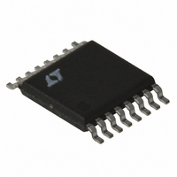
LT1940EFE#TR Linear Technology, LT1940EFE#TR Datasheet - Page 7

LT1940EFE#TR
Manufacturer Part Number
LT1940EFE#TR
Description
IC REG SW DUAL 1.4A STDN 16TSSOP
Manufacturer
Linear Technology
Type
Step-Down (Buck)r
Datasheet
1.LT1940EFEPBF.pdf
(20 pages)
Specifications of LT1940EFE#TR
Internal Switch(s)
Yes
Synchronous Rectifier
No
Number Of Outputs
2
Voltage - Output
1.25 ~ 22 V
Current - Output
1.4A
Frequency - Switching
1.1MHz
Voltage - Input
3.6 ~ 25 V
Operating Temperature
-40°C ~ 85°C
Mounting Type
Surface Mount
Package / Case
16-TSSOP Exposed Pad, 16-eTSSOP, 16-HTSSOP
Lead Free Status / RoHS Status
Contains lead / RoHS non-compliant
Power - Output
-
Available stocks
Company
Part Number
Manufacturer
Quantity
Price
BLOCK DIAGRA
duty cycle of the power switch, the feedback loop controls
the peak current in the switch during each cycle. This
current mode control improves loop dynamics and pro-
vides cycle-by-cycle current limit.
The Block Diagram shows only one of the two switching
regulators. A pulse from the slave oscillator sets the RS
flip-flop and turns on the internal NPN bipolar power
switch. Current in the switch and the external inductor
begins to increase. When this current exceeds a level
determined by the voltage at V
resets the flip-flop, turning off the switch. The current in
the inductor flows through the external Schottky diode,
and begins to decrease. The cycle begins again at the next
pulse from the oscillator. In this way the voltage on the V
pin controls the current through the inductor to the output.
The internal error amplifier regulates the output voltage by
continually adjusting the V
The threshold for switching on the V
active clamp of 1.8V limits the output current. The V
is also clamped to the RUN/SS pin voltage. As the internal
current source charges the external soft-start capacitor,
the current limit increases slowly.
APPLICATIO S I FOR ATIO
FB Resistor Network
The output voltage is programmed with a resistor divider
between the output and the FB pin. Choose the 1%
resistors according to:
R2 should be 10.0k or less to avoid bias current errors.
Reference designators refer to the Block Diagram in
Figure 2.
Input Voltage Range
The minimum input voltage is determined by either the
LT1940’s minimum operating voltage of ~3.5V, or by its
maximum duty cycle. The duty cycle is the fraction of time
that the internal switch is on and is determined by the input
and output voltages:
R1 = R2(V
DC = (V
OUT
OUT
+ V
/1.25 – 1)
D
)/(V
U
IN
– V
W
U
C
pin voltage.
SW
C
, current comparator C1
+ V
W
C
D
)
pin is 0.75V, and an
U
C
pin
C
Each switcher contains an independent oscillator. This
slave oscillator is normally synchronized to the master
oscillator. However, during start-up, short-circuit or over-
load conditions, the FB pin voltage will be near zero and an
internal comparator gates the master oscillator clock
signal. This allows the slave oscillator to run the regulator
at a lower frequency. This frequency foldback behavior
helps to limit switch current and power dissipation under
fault conditions.
The switch driver operates from either the input or from
the BOOST pin. An external capacitor and diode are used
to generate a voltage at the BOOST pin that is higher than
the input supply. This allows the driver to fully saturate the
internal bipolar NPN power switch for efficient operation.
A power good comparator trips when the FB pin is at 90%
of its regulated value. The PG output is an open collector
transistor that is off when the output is in regulation,
allowing an external resistor to pull the PG pin high. Power
good is valid when the LT1940 is enabled (either RUN/SS
pin is high) and V
where V
(~0.4V) and V
(~0.3V at maximum load). This leads to a minimum input
voltage of:
with DC
A more detailed analysis includes inductor loss and the
dependence of the diode and switch drop on operating
current. A common application where the maximum duty
cycle limits the input voltage range is the conversion of
5V to 3.3V. The maximum load current that the LT1940
can deliver at 3.3V depends on the accuracy of the 5V
input supply. With a low loss inductor (DCR less than
80m ), the LT1940 can deliver 1A for V
1.4A for V
V
INMIN
MAX
D
= (V
is the forward voltage drop of the catch diode
IN
= 0.78.
> 4.85V.
SW
OUT
is the voltage drop of the internal switch
IN
+ V
is greater than ~2.4V.
D
)/DC
LT1940/LT1940L
MAX
- V
D
+ V
SW
IN
> 4.7V and
1940fa
7


