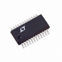
LTC3736EGN-2#PBF Linear Technology, LTC3736EGN-2#PBF Datasheet - Page 6

LTC3736EGN-2#PBF
Manufacturer Part Number
LTC3736EGN-2#PBF
Description
IC CTRLR SW SYNC DUAL 2PH 24SSOP
Manufacturer
Linear Technology
Series
PolyPhase®r
Type
Step-Down (Buck)r
Datasheet
1.LTC3736EGN-2PBF.pdf
(28 pages)
Specifications of LTC3736EGN-2#PBF
Internal Switch(s)
No
Synchronous Rectifier
Yes
Number Of Outputs
2
Voltage - Output
0.6 ~ 9.8 V
Current - Output
1A
Frequency - Switching
550kHz ~ 750kHz
Voltage - Input
2.75 ~ 9.8 V
Operating Temperature
-40°C ~ 85°C
Mounting Type
Surface Mount
Package / Case
24-SSOP
Lead Free Status / RoHS Status
Lead free / RoHS Compliant
Power - Output
-
Available stocks
Company
Part Number
Manufacturer
Quantity
Price
TYPICAL PERFORMANCE CHARACTERISTICS
PIN FUNCTIONS
LTC3736-2
I
Error Amplifi er Compensation Point. Nominal operating
range on these pins is from 0.7V to 2V. The voltage on
these pins determines the threshold of the main current
comparator.
PLLLPF (Pin 3/Pin 6): Frequency Set/PLL Lowpass Filter.
When synchronizing to an external clock, this pin serves as
the lowpass fi lter point for the phase-locked loop. Normally
a series RC is connected between this pin and ground.
When not synchronizing to an external clock, this pin serves
as the frequency select input. Tying this pin to GND selects
300kHz operation; tying this pin to V
operation. Floating this pin selects 550kHz operation.
SGND (Pin 4/Pin 7): Small-Signal Ground. This pin serves
as the ground connection for most internal circuits.
V
powers the entire chip except for the gate drivers. Exter-
nally fi ltering this pin with a lowpass RC network (e.g.,
R = 10Ω, C = 1μF) is suggested to minimize noise pickup,
especially in high load current applications.
TRACK (Pin 6/Pin 9): Tracking Input for Second Controller.
Allows the start-up of V
ing to a ratio established by a resistor divider on V
connected to the TRACK pin. For one-to-one tracking of
V
6
TH1
IN
OUT1
2.50
2.45
2.40
2.35
2.30
2.25
2.20
2.15
2.10
/ I
(Pin 5/Pin 8): Chip Signal Power Supply. This pin
–60
Undervoltage Lockout Threshold
vs Temperature
TH2
and V
–40
(Pins 1, 8/Pins 4, 11): Current Threshold and
–20
OUT2
TEMPERATURE (°C)
0
V
V
IN
during start-up, a resistor divider with
IN
FALLING
RISING
20
OUT2
40
(QFN/SSOP Package)
60
to track that of V
80
37362 G16
100
IN
selects 750kHz
12
20
18
16
14
10
OUT1
8
6
4
0
2
2
Shutdown Quiescent Current
vs Input Voltage
RUN/SS = 0V
accord-
3
OUT1
4
INPUT VOLTAGE (V)
5
6
values equal to those connected to V
be used to connect to TRACK from V
PGOOD (Pin 9/Pin 12): Power Good Output Voltage Moni-
tor Open-Drain Logic Output. This pin is pulled to ground
when the voltage on either feedback pin (V
not within ±13.3% of its nominal set point.
PGND (Pins 12, 16, 20, 25/Pins 15, 19, 23): Power
Ground. These pins serve as the ground connection for
the gate drivers and the negative input to the reverse cur-
rent comparators. The Exposed Pad must be soldered to
PCB ground.
RUN/SS (Pin 14/Pin 17): Run Control Input and Optional
External Soft-Start Input. Forcing this pin below 0.65V shuts
down the chip (both channels). Driving this pin to V
releasing this pin enables the chip, using the chip’s internal
soft-start. An external soft-start can be programmed by
connecting a capacitor between this pin and ground.
TG1/TG2 (Pins 17, 15/Pins 18, 20): Top (PMOS) Gate
Drive Output. These pins drive the gates of the external
P-channel MOSFETs. These pins have an output swing
from PGND to SENSE
SYNC/FCB (Pin 18/Pin 21): This pin performs three func-
tions: 1) auxiliary winding feedback input, 2) external
clock synchronization input for phase-locked loop, and
3) pulse-skipping operation or forced continuous mode
7
8
9
T
37362 G17
A
= 25°C, unless otherwise noted.
10
+
0.9
0.8
0.7
0.6
0.5
0.4
0.3
0.2
0.1
.
0
2
RUN/SS Start-Up Current
vs Input Voltage
RUN/SS = 0V
3
4
INPUT VOLTAGE (V)
FB2
5
OUT1
from V
6
.
7
FB1
OUT2
8
, V
should
FB2
9
37362 G18
37362fb
IN
) is
10
or


