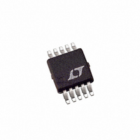
LT3757EMSE#PBF Linear Technology, LT3757EMSE#PBF Datasheet - Page 16

LT3757EMSE#PBF
Manufacturer Part Number
LT3757EMSE#PBF
Description
IC CTRLR DC/DC ADJ 10-MSOP
Manufacturer
Linear Technology
Type
Step-Up (Boost), Inverting, Flyback, Sepicr
Datasheet
1.LT3757EDDPBF.pdf
(36 pages)
Specifications of LT3757EMSE#PBF
Internal Switch(s)
No
Synchronous Rectifier
No
Number Of Outputs
1
Frequency - Switching
100kHz ~ 1MHz
Voltage - Input
2.9 ~ 40 V
Operating Temperature
-40°C ~ 125°C
Mounting Type
Surface Mount
Package / Case
10-MSOP Exposed Pad, 10-HMSOP, 10-eMSOP
Lead Free Status / RoHS Status
Lead free / RoHS Compliant
Current - Output
-
Voltage - Output
-
Power - Output
-
Available stocks
Company
Part Number
Manufacturer
Quantity
Price
applicaTions inForMaTion
LT3757
T
temperature rating. It is recommended to measure the
MOSFET temperature in steady state to ensure that absolute
maximum ratings are not exceeded.
Boost Converter: Output Diode Selection
To maximize efficiency, a fast switching diode with low
forward drop and low reverse leakage is desirable. The
peak reverse voltage that the diode must withstand is
equal to the regulator output voltage plus any additional
ringing across its anode-to-cathode during the on-time.
The average forward current in normal operation is equal
to the output current, and the peak current is equal to:
It is recommended that the peak repetitive reverse voltage
rating V
safety margin is usually sufficient).
The power dissipated by the diode is:
P
and the diode junction temperature is:
T
The R
the R
the board to the ambient temperature in the enclosure. T
must not exceed the diode maximum junction temperature
rating.
J
must not exceed the MOSFET maximum junction
I
D PEAK
J
D
(
= T
= I
θJC
θJA
RRM
O(MAX)
A
for the device plus the thermal resistance from
to be used in this equation normally includes
+ P
)
=
is higher than V
I
L PEAK
D
(
• R
• V
D
θJA
)
=
1
+
OUT
c
2
by a safety margin (a 10V
•
I
L MAX
(
)
J
Boost Converter: Output Capacitor Selection
Contributions of ESR (equivalent series resistance), ESL
(equivalent series inductance) and the bulk capacitance
must be considered when choosing the correct output
capacitors for a given output ripple voltage. The effect of
these three parameters (ESR, ESL and bulk C) on the output
voltage ripple waveform for a typical boost converter is
illustrated in Figure 6.
The choice of component(s) begins with the maximum
acceptable ripple voltage (expressed as a percentage of
the output voltage), and how this ripple should be divided
between the ESR step ∆V
ing ∆V
2% for the maximum output ripple, to be divided equally
between ∆V
change, depending on the requirements of the applica-
tion, and the following equations can easily be modified.
For a 1% contribution to the total ripple voltage, the ESR
of the output capacitor can be determined using the fol-
lowing equation:
Figure 6. The Output Ripple Waveform of a Boost Converter
ESR
COUT
COUT
V
(AC)
OUT
. For the purpose of simplicity, we will choose
ESR
≤
t
ON
0 01
and ∆V
. •
I
D PEAK
(
t
V
OFF
V
ESR
OUT
COUT
)
ESR
V
COUT
. This percentage ripple will
and the charging/discharg-
RINGING DUE TO
TOTAL INDUCTANCE
(BOARD + CAP)
3757 F05
3757fb


