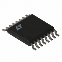
LT1977EFE Linear Technology, LT1977EFE Datasheet - Page 19

LT1977EFE
Manufacturer Part Number
LT1977EFE
Description
IC REG SW 1.5A HV STPDWN 16TSSOP
Manufacturer
Linear Technology
Type
Step-Down (Buck)r
Datasheet
1.LT1977EFEPBF.pdf
(24 pages)
Specifications of LT1977EFE
Internal Switch(s)
Yes
Synchronous Rectifier
No
Number Of Outputs
1
Voltage - Output
1.2 ~ 54 V
Current - Output
1.5A
Frequency - Switching
500kHz
Voltage - Input
3.3 ~ 60 V
Operating Temperature
-40°C ~ 125°C
Mounting Type
Surface Mount
Package / Case
16-TSSOP Exposed Pad, 16-eTSSOP, 16-HTSSOP
Lead Free Status / RoHS Status
Contains lead / RoHS non-compliant
Power - Output
-
Available stocks
Company
Part Number
Manufacturer
Quantity
Price
Part Number:
LT1977EFE
Manufacturer:
LTNEAR
Quantity:
20 000
Company:
Part Number:
LT1977EFE#PBF
Manufacturer:
LT
Quantity:
425
Part Number:
LT1977EFE#PBF
Manufacturer:
LINEAR/凌特
Quantity:
20 000
APPLICATIO S I FOR ATIO
the user to generate a delayed signal after the power good
threshold is exceeded.
Referring to Figure 2, the PGFB pin is the positive input to
a comparator whose negative input is set at V
PGFB is taken above V
the C
the PGFB pin drops below V
100k TO V
500mV/DIV
500mV/DIV
T
2V/DIV
V
pin starting the delay period. When the voltage on
V
SHDN
OUT
V
PG
CT
IN
PG at 80% V
V
OUT
Figure 9. Power Good
LT1977
LT1977
U
PGFB
PGFB
PGFB
Disconnect at 80% V
TIME (10ms/DIV)
with 100ms Delay
V
V
PG
PG
FB
C
FB
C
IN
IN
T
T
U
, current (I
OUT
PGFB
with 100ms Delay
0.27µF
0.27µF
200k
W
the C
CSS
200k
153k
12k
100k
153k
12k
100k
) is sourced into
T
OUT
1977 F09
pin is rapidly
PGFB
C
C
Figure 10. Power Good Circuits
OUT
OUT
U
V
OUT
. When
= 3.3V
V
OUT
= 3.3V
discharged resetting the delay period. The PGFB voltage is
typically generated by a resistive divider from the regu-
lated output or input supply.
The capacitor on the C
delay time between the PGFB pin exceeding its threshold
(V
When the PGFB pin rises above V
(I
voltage on the external capacitor reaches an internal clamp
(V
resultant PG delay time is given by t = C
the voltage on the PGFB pin drops below its V
be discharged rapidly and PG will be active low with a
200µA sink capability. If the SHDN pin is taken below its
threshold during normal operation, the C
discharged and PG inactive, resulting in a non Power Good
cycle when SHDN is taken above its threshold. Figure 9
shows the power good operation with PGFB connected to
FB and the capacitance on C
V
CT
PG at V
OUT
PGFB
CT
) from the C
), the PG pin becomes a high impedance node. The
LT1977
LT1977
Disconnect 3.3V Logic Signal
) and the PG pin set to a high impedance state.
PGFB
PGFB
IN
with 100µs Delay
V
V
PG
PG
FB
C
FB
C
IN
IN
T
T
> 4V with 100ms Delay
T
511k
200k
pin into the external capacitor. When the
0.27µF
270pF
200k
200k
165k
100k
866k
100k
1977 F10
T
pin determines the amount of
T
C
= 0.1µF. The PGOOD pin has
OUT
C
V
OUT
OUT
PGFB
V
= 3.3V
OUT
current is sourced
= 12V
CT
• (V
LT1977
T
PGFB
pin will be
CT
)/(I
, C
19
CT
CT
1977fa
). If
will


