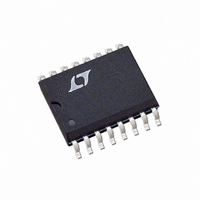
LTC1435CS Linear Technology, LTC1435CS Datasheet - Page 5

LTC1435CS
Manufacturer Part Number
LTC1435CS
Description
IC SW REG SYNC STEP-DOWN 16-SOIC
Manufacturer
Linear Technology
Type
Step-Down (Buck)r
Datasheet
1.LTC1435CGPBF.pdf
(20 pages)
Specifications of LTC1435CS
Internal Switch(s)
No
Synchronous Rectifier
Yes
Number Of Outputs
1
Voltage - Output
1.19 ~ 9 V
Current - Output
50mA
Frequency - Switching
125kHz
Voltage - Input
3.5 ~ 30 V
Operating Temperature
0°C ~ 70°C
Mounting Type
Surface Mount
Package / Case
16-SOIC (3.9mm Width)
Lead Free Status / RoHS Status
Contains lead / RoHS non-compliant
Power - Output
-
Available stocks
Company
Part Number
Manufacturer
Quantity
Price
Part Number:
LTC1435CS
Manufacturer:
LT/凌特
Quantity:
20 000
Part Number:
LTC1435CS#PBF
Manufacturer:
LINEAR/凌特
Quantity:
20 000
Part Number:
LTC1435CS8
Manufacturer:
LT/凌特
Quantity:
20 000
TYPICAL PERFORMANCE CHARACTERISTICS
PIN
C
ground sets the operating frequency.
RUN/SS (Pin 2): Combination of Soft Start and Run
Control Inputs. A capacitor to ground at this pin sets the
ramp time to full current output. The time is approximately
0.5s/ F. Forcing this pin below 1.3V causes the device to
be shut down. In shutdown all functions are disabled.
I
current comparator threshold increases with this control
voltage. Nominal voltage range for this pin is 0V to 2.5V.
SFB (Pin 4): Secondary Winding Feedback Input. Nor-
mally connected to a feedback resistive divider from the
secondary winding. This pin should be tied to: ground to
force continuous operation; INTV
don’t use a secondary winding; and a resistive divider from
the output in applications using a secondary winding.
SGND (Pin 5): Small-Signal Ground. Must be routed
separately from other grounds to the (–) terminal of C
V
external resistive divider across the output.
SENSE
SENSE
Built-in offsets between SENSE
conjunction with R
EXTV
INTV
TH
OSC
OSENSE
U
(Pin 3): Error Amplifier Compensation Point. The
CC
CC
(Pin 1): External capacitor C
FUNCTIONS
–
+
. This switch closes and supplies V
(Pin 9): Input to the Internal Switch Connected to
(Pin 7): The (–) Input to the Current Comparator.
(Pin 8): The (+) Input to the Current Comparator.
(Pin 6): Receives the feedback voltage from an
U
200mV/DIV
20mV/DIV
V
V
OUT
ITH
SENSE
Burst Mode Operation
I
LOAD
U
= 50mA
set the current trip thresholds.
W
–
U
CC
and SENSE
OSC
in applications that
from this pin to
CC
power when-
1435 G16
+
pins in
OUT
.
ever EXTV
in Applications Information section. Do not exceed 10V on
this pin. Connect to V
PGND (Pin 10): Driver Power Ground. Connects to source
of bottom N-channel MOSFET and the (–) terminal of C
BG (Pin 11): High Current Gate Drive for Bottom
N-Channel MOSFET. Voltage swing at this pin is from
ground to INTV
INTV
EXTV
ered from this voltage. Must be closely decoupled to power
ground with a minimum of 2.2 F tantalum or electrolytic
capacitor.
V
to the IC’s signal ground pin.
SW (Pin 14): Switch Node Connection to Inductor. Volt-
age swing at this pin is from a Schottky diode (external)
voltage drop below ground to V
BOOST (Pin 15): Supply to Topside Floating Driver. The
bootstrap capacitor is returned to this pin. Voltage swing
at this pin is from INTV
TG (Pin 16): High Current Gate Drive for Top N-Channel
MOSFET. This is the output of a floating driver with a
voltage swing equal to INTV
switch node voltage SW.
IN
(Pin 13): Main Supply Pin. Must be closely decoupled
CC
INDUCTOR
CC
CURRENT
RUN/SS
5V/DIV
1A/DIV
(Pin 12): Output of the Internal 5V Regulator and
Switch. The driver and control circuits are pow-
CC
Soft Start: Load Current vs Time
is higher than 4.7V. See EXTV
CC
.
OUT
CC
if V
to V
OUT
IN
CC
IN
+ INTV
.
superimposed on the
5V.
1435 G17
CC
LTC1435
.
CC
connection
5
IN
.


