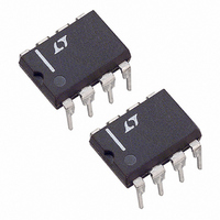
LT1372HVCN8#PBF Linear Technology, LT1372HVCN8#PBF Datasheet

LT1372HVCN8#PBF
Specifications of LT1372HVCN8#PBF
Related parts for LT1372HVCN8#PBF
LT1372HVCN8#PBF Summary of contents
Page 1
... Nonlinear error amplifier transconductance re- duces output overshoot on start-up or overload recovery. Oscillator frequency shifting protects external compo- nents during overload conditions. , LTC and LT are registered trademarks of Linear Technology Corporation. † V OUT 12V R1 53 ...
Page 2
LT1372/LT1377 ABSOLUTE AXI U RATI GS (Note 1) Supply Voltage ....................................................... 30V Switch Voltage LT1372/LT1377 .................................................. 35V LT1372HV .......................................................... 42V S/S Pin Voltage ....................................................... 30V Feedback Pin Voltage (Transient, 10ms) .............. 10V Feedback Pin Current ........................................... 10mA ...
Page 3
ELECTRICAL CHARACTERISTICS The denotes specifcatons which appy over the full operating temperature range, otherwise specifications are 5V 0.6V S/S and NFB pins open, unless otherwise noted ...
Page 4
LT1372/LT1377 W U TYPICAL PERFOR A CE CHARACTERISTICS Shutdown Delay and Threshold vs Temperature SHUTDOWN THRESHOLD SHUTDOWN DELAY –50 100 125 150 – TEMPERATURE ( ...
Page 5
CTIO S V (Pin 1): The compensation pin is used for frequency C compensation, current limiting and soft start the output of the error amplifier and the input of the current comparator. Loop ...
Page 6
... FB pin to 1.245V. This architecture, which uses the same main error amplifier, prevents duplicating functions and maintains ease of use. Consult Linear Technology Market- ing for units that can regulate down to – 1.25V. The error signal developed at the amplifier output is brought out externally ...
Page 7
... U U APPLICATIO S I FOR ATIO Positive fixed voltage versions are available (consult Linear Technology marketing). Negative Output Voltage Setting The LT1372/LT1377 develops a – 2.49V reference (V from the NFB pin to ground. Output voltage is set by connecting the NFB pin to an output resistor divider (Figure 2). The – ...
Page 8
... IN 5. After making an initial choice, consider the secondary things like output voltage ripple, second sourcing, etc. Use the experts in the Linear Technology application department if you feel uncertain about the final choice. They have experience with a wide range of inductor types and can tell you about the latest developments in low profile, surface mounting, etc ...
Page 9
... ESL before ESR becomes effective. They are appropriate for input bypassing because of their high ripple current ratings and tolerance of turn-on surges. Linear Technology plans to issue a Design Note on the use – ceramic capacitors in the near future. ...
Page 10
LT1372/LT1377 U U APPLICATIO S I FOR ATIO Frequency Compensation Loop frequency compensation is performed on the output of the error amplifier (V pin) with a series RC network. C The main pole is formed by the series capacitor and ...
Page 11
... PATENTS MAY APPLY Information furnished by Linear Technology Corporation is believed to be accurate and reliable. However, no responsibility is assumed for its use. Linear Technology Corporation makes no represen- tation that the interconnection of circuits as described herein will not infringe on existing patent rights. N Dual Output Flyback Converter with Overvoltage Protection R2 1 ...
Page 12
... TYP = 1.2V, Synchronizable Up to 2MHz, MSOP Package REF sn13727 13727fbs LT/TP 0401 2K REV B • PRINTED IN THE USA LINEAR TECHNOLOGY CORPORATION 1995 0.150 – 0.157** (3.810 – 3.988) 0.004 – 0.010 (0.101 – 0.254) 0.050 (1.270) ...


