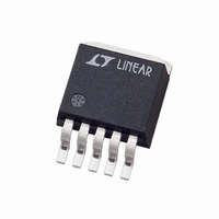
LT1076CQ-5 Linear Technology, LT1076CQ-5 Datasheet - Page 3

LT1076CQ-5
Manufacturer Part Number
LT1076CQ-5
Description
IC SWTCHNG REG STP-DWN 2A 5-DD
Manufacturer
Linear Technology
Type
Step-Down (Buck), Step-Up (Boost), Inverting, Flybackr
Datasheet
1.LT1076CT-5PBF.pdf
(8 pages)
Specifications of LT1076CQ-5
Internal Switch(s)
Yes
Synchronous Rectifier
No
Number Of Outputs
1
Voltage - Output
5V
Current - Output
2A
Frequency - Switching
100kHz
Voltage - Input
8 ~ 45 V
Operating Temperature
0°C ~ 70°C
Mounting Type
Surface Mount
Package / Case
D²Pak, TO-263 (5 leads + tab)
Lead Free Status / RoHS Status
Contains lead / RoHS non-compliant
Power - Output
-
Available stocks
Company
Part Number
Manufacturer
Quantity
Price
Company:
Part Number:
LT1076CQ-5
Manufacturer:
Linear Technology
Quantity:
135
Part Number:
LT1076CQ-5
Manufacturer:
LT
Quantity:
20 000
Part Number:
LT1076CQ-5#PBF
Manufacturer:
LINEAR/凌特
Quantity:
20 000
Part Number:
LT1076CQ-5#TRPBF
Manufacturer:
LINEAR/凌特
Quantity:
20 000
ELECTRICAL CHARACTERISTICS
temperature range, otherwise specifi cations are at T
Note 1: Stresses beyond those listed under Absolute Maximum Ratings
may cause permanent damage to the device. Exposure to any Absolute
Maximum Rating condition for extended periods may affect device
reliability and lifetime.
Note 2: To calculate maximum switch “on” voltage at currents between
low and high conditions, a linear interpolation may be used.
Note 3: A sense pin voltage (V
clamp level and the switch duty cycle to zero. This approximates the zero
load condition where duty cycle approaches zero.
Note 4: Total voltage from V
up for proper regulation. For T
Note 5: Switch frequency is internally scaled down when the sense pin
voltage is less than 2.6V to avoid extremely short switch on times. During
SYMBOL
Supply Current (Note 3)
Minimum Supply Voltage
Switch Current Limit (Note 5)
Maximum Duty Cycle
Switching Frequency
Switching Frequency Line Regulation 8V ≤ V
Error Amplifi er Voltage Gain (Note 8) 1V ≤ V
Error Amplifi er Transconductance
(Note 8)
Error Amplifi er Source and Sink
Current
Sense Pin Divider Resistance
Sense Voltage
Output Voltage Tolerance
Output Voltage Line Regulation
VC Voltage at 0% Duty Cycle
Multiplier Reference Voltage
Shutdown Pin Current
Shutdown Thresholds
Thermal Resistance Junction to Case
IN
SENSE
A
pin to ground pin must be ≥ 8V after start-
< 25°C, limit = 5V.
) of 5.5V forces the VC pin to its low
CONDITIONS
V
40V < V
V
Normal Mode
Start-Up Mode (Note 4)
I
R
R
T
V
Source (V
Sink (V
V
V
All Conditions of Input Voltage, Output Voltage,
Temperature and Load Current
8V ≤ V
Over Temperature
V
V
Switch Duty Cycle = 0
Fully Shut Down
LIM
J
OUT
SHDN
LIM
LIM
OUT
C
OUT
SHDN
SHDN
≤ 125°C
= 2V
= Open
= 10k (Note 10)
= 7k (Note 10)
= 5.5V, V
= V
(Nominal) = 5V
IN
C
IN
= 0.1V (Device Shutdown) (Note 9)
= 5V
≤ V
SENSE
IN
≤ 4V
SENSE
≤ V
≤ V
SENSE
THRESHOLD
< 60V
MAX
MAX
= 5.5V)
IN
= 0V (Note 5)
= 4.5V)
≤ 40V
(Note 8)
(Note 7)
(≅ 2.5V)
J
= 25°C. V
The
l
IN
denotes the specifi cations which apply over the full operating
= 25V, unless otherwise noted.
current limit testing, V
of 1ms.
Note 6: Switch to input voltage limitation must also be observed.
Note 7: V
Note 8: Error amplifi er voltage gain and transconductance are
specifi ed relative to the internal feedback node. To calculate gain and
transconductance from the Sense pin (Output) to the V
0.44.
Note 9: Does not include switch leakage.
Note 10:
MAX
I
LIM
= 40V for the LT1076-5 and 60V for the LT1076HV-5.
≈
R
LIM
5
k
SENSE
− 1
k
is adjusted to give a minimum switch on time
l
l
l
l
l
l
l
l
l
l
l
l
3700
4.85
MIN
100
0.7
2.2
0.1
85
90
85
2
3
5
0.005
2000
5000
0.03
±0.5
±1.0
–4.0
2.45
0.30
TYP
140
100
140
8.5
9.0
7.3
3.5
2.6
1.8
1.2
1.0
1.5
90
20
24
10
5
5
LT1076-5
C
pin, multiply by
8000
MAX
5.15
0.02
300
110
120
225
8.0
4.8
3.2
0.1
1.6
2.7
0.5
11
12
±2
±3
20
50
8
4
UNITS
mV/°C
10765fc
μmho
°C/W
3
%/V
%/V
kHz
kHz
kHz
mA
mA
V/V
mA
kΩ
μA
μA
μA
μA
%
%
%
V
V
A
A
A
V
V
V
V
V


