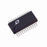
LTC3711EGN Linear Technology, LTC3711EGN Datasheet - Page 19

LTC3711EGN
Manufacturer Part Number
LTC3711EGN
Description
IC SW REG SYNC STPDN 5BIT 24SSOP
Manufacturer
Linear Technology
Type
Step-Down (Buck)r
Datasheet
1.LTC3711EGN.pdf
(24 pages)
Specifications of LTC3711EGN
Internal Switch(s)
No
Synchronous Rectifier
Yes
Number Of Outputs
1
Voltage - Output
0.93 ~ 2 V
Current - Output
2A
Frequency - Switching
Adjustable
Voltage - Input
4 ~ 36 V
Operating Temperature
-40°C ~ 85°C
Mounting Type
Surface Mount
Package / Case
24-SSOP
Lead Free Status / RoHS Status
Contains lead / RoHS non-compliant
Power - Output
-
Available stocks
Company
Part Number
Manufacturer
Quantity
Price
Part Number:
LTC3711EGN
Manufacturer:
LINEAR/凌特
Quantity:
20 000
Part Number:
LTC3711EGN#TRPBF
Manufacturer:
LINEAR/凌特
Quantity:
20 000
APPLICATIO S I FOR ATIO
In the design example, Figure 9, five 0.025 capacitors
are required in parallel to keep the output voltage within
tolerance. Using active voltage positioning, the same
specification can be met with only three capacitors. In this
case, the load step will cause an output voltage change of:
By positioning the output voltage 60mV above the regula-
tion point at no load, it will only drop 65mV below the
regulation point after the load step, well within the 100mV
tolerance.
Implementing active voltage positioning requires setting a
precise gain between the sensed current and the output
voltage. Because of the variability of MOSFET on-resis-
tance, it is prudent to use a sense resistor with active
V
C
C
L1: SUMIDA CEP125-IR0MC-H
IN
OUT
OUT STEP
: UNITED CHEMICON THCR70EIH226ZT
: CORNELL DUBILIER
470pF
0.1 F
(
C
C
SS
C1
20k
)
R
330k
C
R
ON
15
U
C
FB
A
ESRE271M02B
100k
C
100pF
R
100pF
C2
PG
U
3
1
0 025
C2
6.8nF
.
Figure 9. CPU Core Voltage Regulator 1.5V/15A at 300kHz
10
11
12
1
2
3
4
5
6
7
8
9
W
VID2
RUN/SS
V
PGOOD
V
FCB
I
SGND
I
V
V
VID3
TH
ON
ON
RNG
FB
OSENSE
LTC3711
125
SENSE
EXTV
INTV
BOOST
PGND
mV
VID1
VID0
VID4
U
SW
V
BG
TG
CC
CC
IN
+
24
23
22
21
20
19
18
17
16
15
14
13
C
0.33 F
C
4.7 F
C
0.1 F
B
VCC
F
voltage positioning. In order to minimize power lost in this
resistor, a low value is chosen of 0.003 . The nominal
sense voltage will now be:
To maintain a reasonable current limit, the voltage on the
V
sponding to a 50mV nominal sense voltage.
Next, the gain of the LTC3711 error amplifier must be
determined. The change in I
change in the output current is:
CMDSH-3
RNG
D
V
B
SNS(NOM)
I
TH
pin is reduced to its minimum value of 0.5V, corre-
1
R
F
24 0 003
V
12
RNG
= (0.003 )(15A) = 45mV
V
M1
IRF7811A
M2
IRF7811A
.
2
R
SENSE
1 H
15
L1
TH
D1
UPS840
A
I
OUT
voltage for a corresponding
3711 F09
1 08
.
+
V
C
22 F
50V
C
270 F
2V
LTC3711
IN
3
OUT
5
V
7V TO 24V
V
1.5V
15A
IN
OUT
19
3711f


