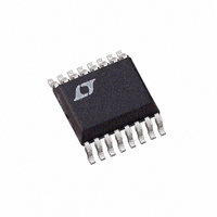
LT1725IGN#PBF Linear Technology, LT1725IGN#PBF Datasheet - Page 21

LT1725IGN#PBF
Manufacturer Part Number
LT1725IGN#PBF
Description
IC CNTRLR ISOLATD FLYBACK 16SSOP
Manufacturer
Linear Technology
Type
Flybackr
Datasheet
1.LT1725ISPBF.pdf
(28 pages)
Specifications of LT1725IGN#PBF
Internal Switch(s)
No
Synchronous Rectifier
No
Number Of Outputs
1
Frequency - Switching
50kHz ~ 250kHz
Operating Temperature
-40°C ~ 125°C
Mounting Type
Surface Mount
Package / Case
16-SSOP
Number Of Pwm Outputs
1
On/off Pin
No
Adjustable Output
No
Topology
Flyback
Switching Freq
90 TO 115kHz
Duty Cycle
90%
Operating Supply Voltage (max)
22V
Synchronous Pin
No
Rise Time
30ns
Fall Time
30ns
Operating Temperature Classification
Automotive
Mounting
Surface Mount
Pin Count
16
Package Type
SSOP N
Lead Free Status / RoHS Status
Lead free / RoHS Compliant
Current - Output
-
Voltage - Output
-
Voltage - Input
-
Power - Output
-
Lead Free Status / Rohs Status
Compliant
Available stocks
Company
Part Number
Manufacturer
Quantity
Price
APPLICATIO S I FOR ATIO
SWITCH NODE CONSIDERATIONS
For maximum efficiency, gate drive rise and fall times are
made as short as practical. To prevent radiation and high
frequency resonance problems, proper layout of the
components connected to the IC is essential, especially
the power paths (primary and secondary). B field (mag-
netic) radiation is minimized by keeping MOSFET leads,
output diode, and output bypass capacitor leads as short
as possible. E field radiation is kept low by minimizing the
length and area of all similar traces. A ground plane
should always be used under the switcher circuitry to
prevent interplane coupling.
The high speed switching current paths are shown sche-
matically in Figure 8. Minimum lead length in these paths
are essential to ensure clean switching and minimal EMI.
The path containing the input capacitor, transformer pri-
mary and MOSFET, and the path containing the trans-
former secondary, output diode and output capacitor
contain “nanosecond” rise and fall times. Keep these
paths as short as possible.
U
U
W
+
Figure 8. High Speed Current Switching Paths
PGND
V
CC
V
CC
U
GATE
DISCHARGE
PATH
GATE
+
GATE DRIVE RESISTOR CONSIDERATIONS
The gate drive circuitry internal to the LT1725 has been
designed to have as low an output impedance as practi-
cally possible—only a few ohms. A strong L/C resonance
is potentially presented by the inductance of the path
leading to the gate of the power MOSFET and its overall
gate capacitance. For this reason the path from the GATE
package pin to the physical MOSFET gate should be kept
as short as possible, and good layout/ground plane prac-
tice used to minimize the parasitic inductance.
An explicit series gate drive resistor may be useful in some
applications to damp out this potential L/C resonance
(typically tens of MHz). A minimum value of perhaps
several ohms is suggested, and higher values (typically a
few tens of ohms) will offer increased damping. However,
as this resistor value becomes too large, gate voltage rise
time will increase to unacceptable levels, and efficiency
will suffer due to the sluggish switching action.
V
IN
PRIMARY
POWER
PATH
SECONDARY
POWER
PATH
+
1725 F08
LT1725
21
1725fa


