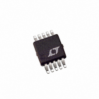
LTC3407EMSE-4#TRPBF Linear Technology, LTC3407EMSE-4#TRPBF Datasheet - Page 7

LTC3407EMSE-4#TRPBF
Manufacturer Part Number
LTC3407EMSE-4#TRPBF
Description
IC REG DC/DC DUAL 1.5MHZ 10-MSOP
Manufacturer
Linear Technology
Type
Step-Down (Buck)r
Datasheet
1.LTC3407EDD-4PBF.pdf
(16 pages)
Specifications of LTC3407EMSE-4#TRPBF
Internal Switch(s)
Yes
Synchronous Rectifier
Yes
Number Of Outputs
2
Voltage - Output
0.6 ~ 5 V
Current - Output
1A
Frequency - Switching
1.5MHz
Voltage - Input
2.5 ~ 5.5 V
Operating Temperature
-40°C ~ 85°C
Mounting Type
Surface Mount
Package / Case
10-MSOP Exposed Pad, 10-HMSOP, 10-eMSOP
Lead Free Status / RoHS Status
Lead free / RoHS Compliant
Power - Output
-
Available stocks
Company
Part Number
Manufacturer
Quantity
Price
OPERATION
decrease causes the error amplifi er to increase the I
voltage until the average inductor current matches the
new load current.
The main control loop is shut down by pulling the RUN
pin to ground.
Low Current Operation
Two modes are available to control the operation of the
LTC3407-4 at low currents. Both modes automatically
switch from continuous operation to the selected mode
when the load current is low.
To optimize effi ciency, the Burst Mode operation can be
selected. When the load is relatively light, the LTC3407-4
automatically switches into Burst Mode operation, in which
the PMOS switch operates intermittently based on load
demand with a fi xed peak inductor current. By running
cycles periodically, the switching losses which are domi-
nated by the gate charge losses of the power MOSFETs
are minimized. The main control loop is interrupted when
the output voltage reaches the desired regulated value.
A hysteretic voltage comparator trips when I
0.35V, shutting off the switch and reducing the power. The
output capacitor and the inductor supply the power to the
load until I
main control loop which starts another cycle.
APPLICATIONS INFORMATION
A general LTC3407-4 application circuit is shown in
Figure 2. External component selection is driven by the
load requirement, and begins with the selection of the
inductor L. Once the inductor is chosen, C
can be selected.
Inductor Selection
Although the inductor does not infl uence the operat-
ing frequency, the inductor value has a direct effect on
ripple current. The inductor ripple current ΔI
with higher inductance and increases with higher V
V
OUT
:
I
L
=
V
f
TH
O
OUT
• L
exceeds 0.65V, turning on the switch and the
• 1–
V
V
OUT
IN
IN
L
TH
decreases
and C
is below
IN
OUT
TH
or
For lower ripple noise at low currents, the pulse-skipping
mode can be used. In this mode, the LTC3407-4 continues
to switch at a constant frequency down to very low cur-
rents, where it will begin skipping pulses. The effi ciency in
pulse-skipping mode can be improved slightly by connect-
ing the SW node to the MODE/SYNC input which reduces
the clock frequency by approximately 30%.
Dropout Operation
When the input supply voltage decreases toward the
output voltage, the duty cycle increases to 100% which
is the dropout condition. In dropout, the PMOS switch is
turned on continuously with the output voltage being equal
to the input voltage minus the voltage drops across the
internal P-channel MOSFET and the inductor.
An important design consideration is that the R
of the P-channel switch increases with decreasing input
supply voltage (See Typical Performance Characteristics).
Therefore, the user should calculate the power dissipation
when the LTC3407-4 is used at 100% duty cycle with low
input voltage (See Thermal Considerations in the Applica-
tions Information Section).
Low Supply Operation
To prevent unstable operation, the LTC3407-4 incorporates
an Under-Voltage Lockout circuit which shuts down the
part when the input voltage drops below about 1.65V.
Accepting larger values of ΔI
inductances, but results in higher output voltage ripple,
greater core losses, and lower output current capability.
A reasonable starting point for setting ripple current is
ΔI
The largest ripple current ΔI
voltage. To guarantee that the ripple current stays below a
specifi ed maximum, the inductor value should be chosen
according to the following equation:
The inductor value will also have an effect on Burst Mode
operation. The transition from low current operation
L
L
= 0.3 • I
f
O
V
OUT
• I
LIM
L
, where I
• 1–
V
IN(MAX)
V
LIM
OUT
is the peak switch current limit.
L
occurs at the maximum input
L
allows the use of low
LTC3407-4
DS(ON)
34074fa
7


