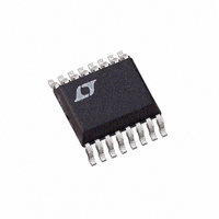
LTC3701EGN Linear Technology, LTC3701EGN Datasheet - Page 16

LTC3701EGN
Manufacturer Part Number
LTC3701EGN
Description
IC DC/DC CNTRLR STPDN DUAL16SSOP
Manufacturer
Linear Technology
Series
PolyPhase®r
Type
Step-Down (Buck)r
Datasheet
1.LTC3701EGN.pdf
(20 pages)
Specifications of LTC3701EGN
Internal Switch(s)
No
Synchronous Rectifier
No
Number Of Outputs
2
Voltage - Output
0.8 ~ 10 V
Current - Output
1A
Frequency - Switching
550kHz
Voltage - Input
2.5 ~ 10 V
Operating Temperature
-40°C ~ 85°C
Mounting Type
Surface Mount
Package / Case
16-SSOP
Lead Free Status / RoHS Status
Contains lead / RoHS non-compliant
Power - Output
-
Available stocks
Company
Part Number
Manufacturer
Quantity
Price
Part Number:
LTC3701EGN
Manufacturer:
LINEAR/凌特
Quantity:
20 000
Part Number:
LTC3701EGN#PBF
Manufacturer:
LT/凌特
Quantity:
20 000
Part Number:
LTC3701EGN#TR
Manufacturer:
LT/凌特
Quantity:
20 000
Part Number:
LTC3701EGN#TRPBF
Manufacturer:
LT/凌特
Quantity:
20 000
Company:
Part Number:
LTC3701EGNPBF
Manufacturer:
LINEAR
Quantity:
1 306
LTC3701
APPLICATIO S I FOR ATIO
2) Are the signal and power grounds kept separate? The
LTC3701 signal ground consists of the feedback resistor
divider, the I
The power ground consists of the (–) terminal of C
(–) terminals of C
diodes, and Pin 13 of the LTC3701. The power ground
traces should be kept short, direct, and wide. Connect the
anode of the Schottky diodes directly to the input capacitor
ground.
3) Do the V
resistors? Put the feedback resistors close to the V
The traces connecting the top feedback resistors to the
corresponding output capacitor should to be Kelvin traces.
4) Are the SENSE
minimum PC trace spacing? The (optional) filter capacitor
between SENSE
possible to the IC. Ensure accurate current sensing with
Kelvin connections at the sense resistor.
5) Keep the switching nodes (SW1, SW2) and top gate
nodes (PGATE1, PGATE2) away from small-signal nodes,
especially the opposite channel’s voltage and current
sensing feedback pins. All of these nodes have large and
fast moving signals and therefore should be keep on the
“output side” of the LTC3701 and occupy minimum PC
trace area.
Design Example
As a design example for one channel, assume V
operating from a maximum of 4.2V down to a minimum of
2.7V. Load current requirement is a maximum of 1.5A , but
most of the time it will be in a standby mode requiring only
2mA. Efficiency at both low and high load currents is
important. Burst Mode operation at light loads is desired.
Output voltage is 2.5V.
16
Maximum Duty Cycle =
TH
FB
/RUN compensation network, and Pin 4.
+
pins connect directly to the feedback
–
and SENSE
and SENSE
OUT1,2
U
, the anodes of the Schottky
U
+
V
–
IN MIN
leads routed together with
V
OUT
(
should be as close as
W
)
V
D
V
D
U
93
IN
FB
%
will be
IN
pins.
, the
From Figure 2, SF = 57%.
In the application, a 0.03 resistor is used. The PLLLPF
pin will be left floating, so the LTC3701 will operate at its
default frequency of 550kHz. For continuous operation in
Burst Mode, the required minimum inductor value is:
For the selection of the external MOSFET, the R
must be guaranteed at 2.5V since the LTC3701 has to work
down to 2.7V. Let’s assume that the MOSFET dissipation
is to be limited to P
is 50 C/W. Hence, the junction temperature at T
will be 37.5 C and p = 0.005 • (37.5 – 25) = 0.0625. The
required R
The P-channel MOSFET requirement can be met by an
Si3443DV.
The requirement for the Schottky diode is the most strin-
gent when V
R
Schottky is 0.1/0.03 = 3.3A. An MBRS340T3 Schottky
diode is chosen. With 3.3A flowing through, the diode is
rated with a forward voltage of 0.4V. Therefore, the worst-
case power dissipated by the diode is 1.32W. The addition
of D
tion to approximately 0.66W
The input capacitor requires an RMS current rating of at
least 0.75A at temperature, and C
of 0.1 for optimum efficiency.
SENSE
R
L
R
FB1
MIN
SENSE
DS ON
(
and D
resistor, the short-circuit current through the
)
DS(ON)
550
OUT
12 7
FB2
4 2
DC I
kHz
.
. •
V
(Figure 6) will reduce the diode dissipa-
is then given by:
•
= 0V, i.e., short circuit. With a 0.03
P
– .
OUT
I
SF
OUT
0 03
0 03
= 250mW and its thermal resistance
2 5
P
.
.
P
2
V
•
1
V
100
p
2 5
4 2
.
.
12 7 1 5
OUT
V
V
0 11
0 57
. • .
.
.
will require an ESR
0 3
0 3
.
.
V
V
0 03
.
2 00
A
.
= 25 C
DS(ON)
3701fa
H


