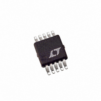
LTC3407EMSE-4#PBF Linear Technology, LTC3407EMSE-4#PBF Datasheet - Page 3

LTC3407EMSE-4#PBF
Manufacturer Part Number
LTC3407EMSE-4#PBF
Description
IC REG DC/DC DUAL 1.5MHZ 10-MSOP
Manufacturer
Linear Technology
Type
Step-Down (Buck)r
Datasheet
1.LTC3407EDD-4PBF.pdf
(16 pages)
Specifications of LTC3407EMSE-4#PBF
Internal Switch(s)
Yes
Synchronous Rectifier
Yes
Number Of Outputs
2
Voltage - Output
0.6 ~ 5 V
Current - Output
1A
Frequency - Switching
1.5MHz
Voltage - Input
2.5 ~ 5.5 V
Operating Temperature
-40°C ~ 85°C
Mounting Type
Surface Mount
Package / Case
10-MSOP Exposed Pad, 10-HMSOP, 10-eMSOP
Lead Free Status / RoHS Status
Lead free / RoHS Compliant
Power - Output
-
Available stocks
Company
Part Number
Manufacturer
Quantity
Price
200mA/DIV
20mV/DIV
ELECTRICAL CHARACTERISTICS
temperature range, otherwise specifi cations are at T
SYMBOL
f
f
I
R
I
POR
V
I
V
Note 1: Stresses beyond those listed under Absolute Maximum Ratings
may cause permanent damage to the device. Exposure to any Absolute
Maximum Rating condition for extended periods may affect device
reliability and lifetime. Pins of regulators should not exceed 6V
Note 2: The LTC3407E-4 is guaranteed to meet specifi ed performance
from 0°C to 85°C. Specifi cations over the –40°C to 85°C operating
temperature range are assured by design, characterization and correlation
with statistical process controls.
TYPICAL PERFORMANCE CHARACTERISTICS
OSC
SYNC
LIM
SW(LKG)
RUN
RUN
MODE
DS(ON)
5V/DIV
V
OUT
SW
I
L
Burst Mode Operation
V
V
I
LOAD
IN
OUT
= 3.6V
= 1.8V
= 100mA
PARAMETER
Oscillator Frequency
Synchronization Frequency
Peak Switch Current Limit
Top Switch On-Resistance
Bottom Switch On-Resistance
Switch Leakage Current
Power-On Reset Threshold
Power-On Reset On-Resistance
Power-On Reset Delay
RUN Threshold
RUN Leakage Current
MODE Threshold Low
MODE Threshold High
2μs/DIV
34073 G01
200mA/DIV
20mV/DIV
5V/DIV
CONDITIONS
V
V
V
(Note 6)
(Note 6)
V
V
V
OUT
SW
FBX
IN
IN
FBX
FBX
I
L
A
= 3V, V
= 5V, V
Pulse-Skipping Mode
V
V
I
= 0.6V
Ramping Up, MODE/SYNC = 0V
Ramping Down, MODE/SYNC = 0V
LOAD
= 25°C. V
IN
OUT
= 3.6V
= 1.8V
= 20mA
FBX
RUN
The
= 0.5V, Duty Cycle <35%
= 0V, V
l
IN
denotes the specifi cations which apply over the full operating
= 3.6V, unless otherwise specifi ed. (Note 2)
1μs/DIV
FBX
Note 3: The LTC3407-4 is tested in a proprietary test mode that connects
V
Note 4: Dynamic supply current is higher due to the internal gate charge
being delivered at the switching frequency.
Note 5: T
according to the following formula: T
Note 6: The DFN switch on-resistance is guaranteed by correlation to
wafer level measurements.
FB
= 0V
to the output of the error amplifi er.
J
is calculated from the ambient T
34073 G02
T
A
= 25°C unless otherwise specifi ed.
●
●
●
500mA/DIV
500mA/DIV
200mV/DIV
I
V
LOAD
V
OUT
IN
I
0.95
MIN
L
1.8
0.3
0
– 0.5
Load Step
V
V
I
LOAD
IN
OUT
J
= 3.6V
= T
= 1.8V
= 80mA ~ 800mA
A
A
+ (P
and power dissipation P
65536
2.25
2.25
0.35
0.30
0.01
–8.5
0.01
TYP
100
1.2
8.5
LTC3407-4
1
D
• θ
10μs/DIV
JA
).
MAX
0.45
0.45
200
2.7
1.6
1.5
0.5
V
1
1
IN
34074 G03
UNITS
Cycles
D
34074fa
3
MHz
MHz
μA
μA
%
%
Ω
Ω
Ω
A
V
V
V


