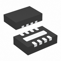
LT3470AIDDB#TRPBF Linear Technology, LT3470AIDDB#TRPBF Datasheet - Page 12

LT3470AIDDB#TRPBF
Manufacturer Part Number
LT3470AIDDB#TRPBF
Description
IC BUCK ADJ .25A 8DFN
Manufacturer
Linear Technology
Type
Step-Down (Buck)r
Datasheet
1.LT3470AEDDBTRMPBF.pdf
(20 pages)
Specifications of LT3470AIDDB#TRPBF
Internal Switch(s)
Yes
Synchronous Rectifier
No
Number Of Outputs
1
Voltage - Output
1.25 ~ 16 V
Current - Output
250mA
Voltage - Input
4 ~ 40 V
Operating Temperature
-40°C ~ 125°C
Mounting Type
Surface Mount
Package / Case
8-DFN
Lead Free Status / RoHS Status
Lead free / RoHS Compliant
Power - Output
-
Frequency - Switching
-
Available stocks
Company
Part Number
Manufacturer
Quantity
Price
APPLICATIONS INFORMATION
LT3470A
(Figure 2b). The circuit in Figure 2a is more efficient
because the BOOST pin current and BIAS pin quiescent
current comes from a lower voltage source. You must also
be sure that the maximum voltage ratings of the BOOST
and BIAS pins are not exceeded.
The LT3470A monitors the boost capacitor for sufficient
voltage such that the switch is allowed to fully saturate.
When boost voltage falls below adequate levels (1.8V
typical) the switch will operate with about 1V of drop, and
an internal current source will begin to pull 50mA (typi-
cal) from the BIAS pin which is typically connected to the
output. This current forces the LT3470A to switch more
often and with more inductor current, which recharges
12
Figure 3. The Minimum Input Voltage Depends on Output
Voltage, Load Current and Boost Circuit
6.0
5.5
5.0
4.5
4.0
3.5
3.0
8
6
5
4
7
Minimum Input Voltage, V
0
Minimum Input Voltage, V
0
T
T
A
A
= 25°C
= 25°C
V
IN
V
50
50
IN
TO RUN/START
TO RUN/START
LOAD CURRENT (mA)
LOAD CURRENT (mA)
100
100
150
150
OUT
200
OUT
200
= 3.3V
3470a F03a
3470a F03b
= 5V
250
250
the boost capacitor. When the boost capacitor voltage is
above 1.8V (typical) the current source turns off, and the
part may enter BurstMode. This cycle will repeat anytime
there is an undervoltage condition on the boost capaci-
tor. See Figure 3 for minimum input voltage for outputs
of 3.3V and 5V.
Shorted Input Protection
If the inductor is chosen so that it won’t saturate exces-
sively at the top switch current limit maximum of 525mA,
an LT3470A buck regulator will tolerate a shorted output
even if V
in systems where the output will be held high when the
input to the LT3470A is absent. This may occur in battery
charging applications or in battery backup systems where
a battery or some other supply is diode OR-ed with the
LT3470A’s output. If the V
SHDN pin is held high (either by a logic signal or because
it is tied to V
pull its quiescent current through its SW pin. This is fine
if your system can tolerate a few mA in this state. If you
ground the SHDN pin, the SW pin current will drop to es-
sentially zero. However, if the V
the output is held high, then parasitic diodes inside the
LT3470A can pull large currents from the output through
the SW pin and the V
will run only when the input voltage is present and that
protects against a shorted or reversed input.
Figure 4. Diode D1 Prevents a Shorted Input from Discharging
a Backup Battery Tied to the Output; It Also Protects the Circuit
from a Reversed Input. The LT3470A Runs Only When the Input is
Present Hot-Plugging Safely
V
IN
1M
100k
IN
D1
= 40V. There is another situation to consider
IN
), then the LT3470A’s internal circuitry will
SHDN
V
IN
LT3470A
GND
IN
BOOST
pin. Figure 4 shows a circuit that
BIAS
SW
IN
FB
pin is allowed to float and the
IN
pin is grounded while
3470a F04
BACKUP
V
OUT
3470afb


