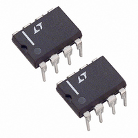
LT1302CN8-5 Linear Technology, LT1302CN8-5 Datasheet - Page 12

LT1302CN8-5
Manufacturer Part Number
LT1302CN8-5
Description
IC DC/DC CONV STEP-UP 5V 8-DIP
Manufacturer
Linear Technology
Type
Step-Up (Boost)r
Datasheet
1.LT1302CS8-5PBF.pdf
(16 pages)
Specifications of LT1302CN8-5
Internal Switch(s)
Yes
Synchronous Rectifier
No
Number Of Outputs
1
Voltage - Output
5V
Current - Output
600mA
Frequency - Switching
220kHz
Voltage - Input
2 ~ 8 V
Operating Temperature
0°C ~ 70°C
Mounting Type
Through Hole
Package / Case
8-DIP (0.300", 7.62mm)
Power - Output
700mW
Lead Free Status / RoHS Status
Contains lead / RoHS non-compliant
Available stocks
Company
Part Number
Manufacturer
Quantity
Price
Part Number:
LT1302CN8-5#PBF
Manufacturer:
LINEAR/凌特
Quantity:
20 000
LT1302/LT1302-5
APPLICATIONS
separate ground trace up under the package as shown.
The battery and load return should go to the power side of
the ground copper.
Thermal Considerations
The LT1302 contains a thermal shutdown feature which
protects against excessive internal (junction) tempera-
ture. If the junction temperature of the device exceeds the
protection threshold, the device will begin cycling be-
tween normal operation and an off state. The cycling is not
harmful to the part. The thermal cycling occurs at a slow
rate, typically 10ms to several seconds, which depends on
the power dissipation and the thermal time constants of
the package and heat sinking. Raising the ambient tem-
perature until the device begins thermal shutdown gives a
good indication of how much margin there is in the
thermal design.
For surface mount devices heat sinking is accomplished
by using the heat spreading capabilities of the PC board
and its copper traces. Experiments have shown that the
heat spreading copper layer does not need to be electri-
cally connected to the tab of the device. The PCB material
can be very effective at transmitting heat between the pad
area attached to pins 1 and 8 of the device, and a ground
or power plane layer either inside or on the opposite side
of the board. Although the actual thermal resistance of the
PCB material is high, the length/area ratio of the thermal
resistance between the layer is small. Copper board stiff-
eners and plated through holes can also be used to spread
the heat generated by the device.
Table 3 lists thermal resistance for the SO package.
Measured values of thermal resistance for several differ-
ent board sizes and copper areas are listed for each
surface mount package. All measurements were taken in
still air on 3/32
be used as a rough guideline in estimating thermal resis-
tance. The thermal resistance for each application will be
affected by thermal interactions with other components as
well as board size and shape.
12
"
FR-4 board with 1oz copper. This data can
U
INFORMATION
U
W
U
Table 3. S8 Package, 8-Lead Plastic SO
TOPSIDE*
2500 sq. mm 2500 sq. mm 2500 sq. mm
1000 sq. mm 2500 sq. mm 2500 sq. mm
225 sq. mm
100 sq. mm
100 sq. mm
100 sq. mm
100 sq. mm
* Pins 1 and 8 attached to topside copper
Calculating Temperature Rise
Power dissipation internal to the LT1302 in a boost
regulator configuration is approximately equal to:
The first term in this equation is due to switch “on-
resistance.” The second term is from the switch driver. R
is switch resistance, typically 0.15 . V
forward drop.
The temperature rise can be calculated from:
where:
P
N8 Package, 8-Lead DIP:
Thermal Resistance (Junction-to-Ambient) = 100 C/W
D
P
I
OUT
JA
T = P
T = Temperature Rise
D
COPPER AREA
I
= Device Power Dissipation
= Thermal Resistance (Junction-to-Ambient)
2
OUT
V
D
OUT
R
2500 sq. mm 2500 sq. mm
2500 sq. mm 2500 sq. mm
1000 sq. mm 2500 sq. mm
225 sq. mm
100 sq. mm
27
BACKSIDE
V
JA
IN
V
D
V
OUT
I
OUT OUT
V
IN
BOARD AREA
2500 sq. mm
2500 sq. mm
V
V
V
IN
D
R
2
(JUNCTION-TO-AMBIENT)
THERMAL RESISTANCE
V
IN
V
D
OUT
I
60 C/W
62 C/W
65 C/W
69 C/W
73 C/W
80 C/W
83 C/W
is the diode
OUT OUT
V
V
V
IN
D
R


