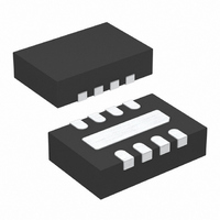
LTC3561EDD#TRPBF Linear Technology, LTC3561EDD#TRPBF Datasheet

LTC3561EDD#TRPBF
Specifications of LTC3561EDD#TRPBF
Available stocks
Related parts for LTC3561EDD#TRPBF
LTC3561EDD#TRPBF Summary of contents
Page 1
... The no-load quiescent current is only 240µA. In shutdown, the device draws <1µA. , LT, LTC and LTM are registered trademarks of Linear Technology Corporation. All other trademarks are the property of their respective owners. Protected by U.S. Patents, including 5481178, 6127815, 6304066, 6498466, 6580258, 6611131. ...
Page 2
LTC3561 ABSOLUTE AXI U RATI GS (Note Voltages .....................................– 0. SHDN/R Voltages ................ – 0. Voltage ................................................– 0. ...
Page 3
ELECTRICAL CHARACTERISTICS Note calculated from the ambient T and power dissipation according to the following formula: LTC3561EDD • 43°C/ Note 6: Switch on-resistance is guaranteed by ...
Page 4
LTC3561 W U TYPICAL PERFOR A CE CHARACTERISTICS Frequency Variation vs Temperature –2 –4 –6 –8 –10 –50 – 100 TEMPERATURE (°C) 3561 G10 CTIO ...
Page 5
W BLOCK DIAGRA 0.8V REFERENCE OPERATIO The LTC3561 uses a constant frequency, current mode architecture. The operating frequency is determined by the value of the R resistor. T The output voltage is set ...
Page 6
LTC3561 U U APPLICATIO S I FOR ATIO A general LTC3561 application circuit is shown in Figure 4. External component selection is driven by the load requirement, and begins with the selection of the inductor L1. Once L1 is chosen, ...
Page 7
U U APPLICATIO S I FOR ATIO Table 1. Representative Surface Mount Inductors MANU- FACTURER PART NUMBER VALUE CURRENT DCR HEIGHT Toko A914BYW-2R2M-D52LC 2.2µH Coilcraft D01608C-222 2.2µH Coilcraft LP01704-222M 2.2µH Sumida CDRH2D18/HP-2R2 2.2µH Taiyo Yuden N05DB2R2M 2.2µH Murata LQN6C2R2M04 2.2µH ...
Page 8
LTC3561 U U APPLICATIO S I FOR ATIO piezoelectric effects. In addition, the high Q of ceramic capacitors along with trace inductance can lead to signifi- cant ringing. Other capacitor types include the Panasonic specialty polymer (SP) capacitors. In most ...
Page 9
U U APPLICATIO S I FOR ATIO reduces surge currents from V by gradually increasing IN the peak inductor current. Power supply sequencing can also be accomplished using this pin. The LTC3561 has an internal digital soft-start which steps up ...
Page 10
LTC3561 U U APPLICATIO S I FOR ATIO The output voltage settling behavior is related to the stability of the closed-loop system and will demonstrate the actual overall supply performance. For a detailed explanation of optimizing the compensation components, including ...
Page 11
U U APPLICATIO S I FOR ATIO looking into the SW pin is a function of both top and bottom MOSFET R and the duty cycle (DC) as DS(ON) follows TOP)(DC DS(ON) The R ...
Page 12
LTC3561 U U APPLICATIO S I FOR ATIO For cost reasons, a ceramic capacitor will be used. C selection is then based on load step droop instead of ESR requirements. For a 5% output droop ≈ ...
Page 13
U TYPICAL APPLICATIO 2.63V TO C1 5.5V 10µ LTC3561 SHDN SGND PGND R3 13k C3 1000pF NOTE: IN DROPOUT, THE OUTPUT TRACKS THE INPUT VOLTAGE C1, C2: ...
Page 14
LTC3561 U TYPICAL APPLICATIO 4.7µH LTC3402 SHDN V OUT + 2 CELLS MODE/SYNC FB PGOOD 10µF R GND T 49.9k C1: TAIYO YUDEN JMK212BJ106MG 0 = ...
Page 15
... RECOMMENDED SOLDER PAD PITCH AND DIMENSIONS Information furnished by Linear Technology Corporation is believed to be accurate and reliable. However, no responsibility is assumed for its use. Linear Technology Corporation makes no represen- tation that the interconnection of its circuits as described herein will not infringe on existing patent rights. ...
Page 16
... LTC3413 3A (I Sink/Source) 2MHz Monolithic Synchronous Regulator OUT for DDR/QDR Memory Termination LTC3440 600mA (I ) 2MHz Synchronous Buck-Boost DC/DC Converter OUT ThinSOT is a trademark of Linear Technology Corporation. Linear Technology Corporation 16 1630 McCarthy Blvd., Milpitas, CA 95035-7417 (408) 432-1900 FAX: (408) 434-0507 ● V OUT 1 ...


