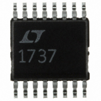
LT1737CGN#PBF Linear Technology, LT1737CGN#PBF Datasheet - Page 18

LT1737CGN#PBF
Manufacturer Part Number
LT1737CGN#PBF
Description
IC CTRLR ISOLATED FLYBACK 16SSOP
Manufacturer
Linear Technology
Type
Flybackr
Datasheet
1.LT1737IGNPBF.pdf
(28 pages)
Specifications of LT1737CGN#PBF
Internal Switch(s)
No
Synchronous Rectifier
No
Number Of Outputs
1
Frequency - Switching
50kHz ~ 250kHz
Voltage - Input
4.1 ~ 20 V
Operating Temperature
0°C ~ 100°C
Mounting Type
Surface Mount
Package / Case
16-SSOP
Primary Input Voltage
20V
No. Of Outputs
1
Output Voltage
12.1V
Output Current
100mA
No. Of Pins
16
Operating Temperature Range
0°C To +100°C
Msl
MSL 1 - Unlimited
Rohs Compliant
Yes
Lead Free Status / RoHS Status
Lead free / RoHS Compliant
Current - Output
-
Voltage - Output
-
Power - Output
-
Available stocks
Company
Part Number
Manufacturer
Quantity
Price
APPLICATIO S I FOR ATIO
LT1737
Output Impedance Error
An additional error source is caused by transformer sec-
ondary current flow through the real life nonzero imped-
ances of the output rectifier, transformer secondary and
output capacitor. Because the secondary current only
flows during the off portion of the duty cycle, the effective
output impedance equals the “DC” lumped secondary
impedance times the inverse of the off duty cycle. If the
output load current remains relatively constant, or, in less
critical applications, the error may be judged acceptable
and the feedback resistor divider ratio adjusted for nomi-
nal expected error. In more demanding applications, out-
put impedance error may be minimized by the use of the
load compensation function (see Load Compensation).
MINIMUM LOAD CONSIDERATIONS
The LT1737 generally provides better low load perfor-
mance than previous generation switcher/controllers uti-
lizing indirect output voltage sensing techniques.
Specifically, it contains circuitry to detect flyback pulse
“collapse,” thereby supporting operation well into discon-
tinuous mode. Nevertheless, there still remain constraints
to ultimate low load operation. These relate to the mini-
mum switch on time and the minimum enable time.
Discontinuous mode operation will be assumed in the
following theoretical derivations.
As outlined in the Operation section, the LT1737 utilizes a
minimum output switch on time, t
combined with expected V
yield an expression for minimum delivered power.
This expression then yields a minimum output current
constraint:
18
Minimum Power
I
OUT MIN
(
)
=
2
1
⎛
⎜
⎝
L
U
PRI
=
=
V
•
2
1
f
OUT
V
⎛
⎜
⎝
U
OUT
L
IN
PRI
f
•
and switching frequency to
I
⎞
⎟
⎠
OUT
⎞
⎟
⎠
(
(
V
V
IN
IN
W
ON
•
•
t
. This value can be
ON
t
ON
)
2
)
2
where
U
An additional constraint has to do with the minimum
enable time. The LT1737 derives its output voltage infor-
mation from the flyback pulse. If the internal minimum
enable time pulse extends beyond the flyback pulse, loss
of regulation will occur. The onset of this condition can be
determined by setting the width of the flyback pulse equal
to the sum of the flyback enable delay, t
minimum enable time, t
the load is then:
Which yields a minimum output constraint:
Note that generally, depending on the particulars of input
and output voltages and transformer inductance, one of
the above constraints will prove more restrictive. In other
words, the minimum load current in a particular applica-
tion will be either “output switch minimum on time”
constrained, or “minimum flyback pulse time” constrained.
(A final note—L
tance as seen from the primary or secondary side respec-
tively. This general treatment allows these expressions to
be used when the transformer turns ratio is nonunity.)
f = switching frequency
L
V
V
t
f = switching frequency
L
V
t
t
I
Minimum Power
ON
ED
EN
OUT MIN
PRI
SEC
IN
OUT
OUT
= enable delay time
= minimum enable time
(
= input voltage
= output switch minimum on time
= transformer primary side inductance
= transformer secondary side inductance
= output voltage
= output voltage
)
=
2
1
PRI
⎛
⎜
⎝
f V
•
L
and L
=
=
SEC
OUT
V
2
1
EN
OUT
⎛
⎜
⎝
SEC
. Minimum power delivered to
L
⎞
⎟
⎠
SEC
(
f
t
•
refer to transformer induc-
ED
I
OUT
⎞
⎟
⎠
+
[
V
t
OUT
EN
)
2
•
where
(
t
EN
ED
+
, plus the
t
ED
)
]
1737fa
2


