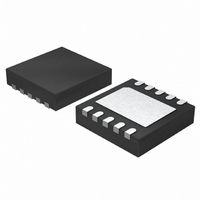
LTC3407EDD Linear Technology, LTC3407EDD Datasheet - Page 10

LTC3407EDD
Manufacturer Part Number
LTC3407EDD
Description
IC REG DC/DC DUAL STEPDOWN 10DFN
Manufacturer
Linear Technology
Type
Step-Down (Buck)r
Datasheet
1.LTC3407EMSE.pdf
(16 pages)
Specifications of LTC3407EDD
Internal Switch(s)
Yes
Synchronous Rectifier
Yes
Number Of Outputs
2
Voltage - Output
0.6 ~ 5 V
Current - Output
1A
Frequency - Switching
1.5MHz
Voltage - Input
2.5 ~ 5.5 V
Operating Temperature
-40°C ~ 85°C
Mounting Type
Surface Mount
Package / Case
10-DFN
Lead Free Status / RoHS Status
Contains lead / RoHS non-compliant
Power - Output
-
Available stocks
Company
Part Number
Manufacturer
Quantity
Price
Company:
Part Number:
LTC3407EDD
Manufacturer:
LT
Quantity:
10 000
Part Number:
LTC3407EDD
Manufacturer:
LT
Quantity:
20 000
Company:
Part Number:
LTC3407EDD#PBF
Manufacturer:
LT
Quantity:
1 730
Part Number:
LTC3407EDD#PBF
Manufacturer:
LT/凌特
Quantity:
20 000
Company:
Part Number:
LTC3407EDD#TR
Manufacturer:
LTC
Quantity:
622
Part Number:
LTC3407EDD#TRPBF
Manufacturer:
LINEAR/凌特
Quantity:
20 000
Company:
Part Number:
LTC3407EDD-1
Manufacturer:
LT
Quantity:
10 000
Company:
Part Number:
LTC3407EDD-2
Manufacturer:
LT
Quantity:
10 000
Part Number:
LTC3407EDD-2
Manufacturer:
LINEAR/凌特
Quantity:
20 000
Part Number:
LTC3407EDD-2#PBF
Manufacturer:
LT/凌特
Quantity:
20 000
APPLICATIONS INFORMATION
LTC3407
Keeping the current small (<5μA) in these resistors maxi-
mizes effi ciency, but making them too small may allow
stray capacitance to cause noise problems and reduce the
phase margin of the error amp loop.
To improve the frequency response, a feed-forward capaci-
tor C
route the V
inductor or the SW line.
Power-On Reset
The POR pin is an open-drain output which pulls low when
either regulator is out of regulation. When both output volt-
ages are within ±8.5% of regulation, a timer is started which
releases POR after 2
delay can be signifi cantly longer in Burst Mode operation
with low load currents, since the clock cycles only occur
during a burst and there could be milliseconds of time
between bursts. This can be bypassed by tying the POR
output to the MODE/SYNC input, to force pulse-skipping
mode during a reset. In addition, if the output voltage
faults during Burst Mode sleep, POR could have a slight
delay for an undervoltage output condition and may not
respond to an overvoltage output. This can be avoided by
using pulse-skipping mode instead. When either channel
is shut down, the POR output is pulled low, since one or
both of the channels are not in regulation.
Mode Selection & Frequency Synchronization
The MODE/SYNC pin is a multipurpose pin which provides
mode selection and frequency synchronization. Connect-
ing this pin to V
provides the best low current effi ciency at the cost of a
higher output voltage ripple. When this pin is connected
to ground, pulse-skipping operation is selected which
provides the lowest output ripple, at the cost of low cur-
rent effi ciency.
The LTC3407 can also be synchronized to another LTC3407
by the MODE/SYNC pin. During synchronization, the mode
is set to pulse-skipping and the top switch turn-on is syn-
chronized to the rising edge of the external clock.
10
V
OUT
F
may also be used. Great care should be taken to
= 0.6V 1+
FB
line away from noise sources, such as the
⎛
⎜
⎝
IN
enables Burst Mode operation, which
R2
R1
18
⎞
⎟
⎠
clock cycles (about 175ms). This
Checking Transient Response
The regulator loop response can be checked by looking
at the load transient response. Switching regulators take
several cycles to respond to a step in load current. When
a load step occurs, V
equal to ΔI
resistance of C
charge C
regulator to return V
this recovery time, V
or ringing that would indicate a stability problem.
The initial output voltage step may not be within the
bandwidth of the feedback loop, so the standard second-
order overshoot/DC ratio cannot be used to determine
phase margin. In addition, a feed-forward capacitor, C
can be added to improve the high frequency response, as
shown in Figure 2. Capacitor C
creating a high frequency zero with R2 which improves
the phase margin.
The output voltage settling behavior is related to the stability
of the closed-loop system and will demonstrate the actual
overall supply performance. For a detailed explanation of
optimizing the compensation components, including a re-
view of control loop theory, refer to Application Note 76.
In some applications, a more severe transient can be caused
by switching in loads with large (>1μF) input capacitors.
The discharged input capacitors are effectively put in paral-
lel with C
can deliver enough current to prevent this problem, if the
switch connecting the load has low resistance and is driven
quickly. The solution is to limit the turn-on speed of the
load switch driver. A Hot Swap™ controller is designed
specifi cally for this purpose and usually incorporates cur-
rent limiting, short-circuit protection, and soft-starting.
Effi ciency Considerations
The percent effi ciency of a switching regulator is equal to
the output power divided by the input power times 100%.
It is often useful to analyze individual losses to determine
what is limiting the effi ciency and which change would
Hot Swap is a trademark of Linear Technology Corporation.
OUT
OUT
LOAD
generating a feedback error signal used by the
, causing a rapid drop in V
OUT
• ESR, where ESR is the effective series
. ΔI
OUT
OUT
OUT
LOAD
immediately shifts by an amount
to its steady-state value. During
can be monitored for overshoot
also begins to charge or dis-
F
provides phase lead by
OUT
. No regulator
3407fa
F
,


