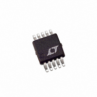
LT1310EMSE Linear Technology, LT1310EMSE Datasheet

LT1310EMSE
Specifications of LT1310EMSE
Available stocks
Related parts for LT1310EMSE
LT1310EMSE Summary of contents
Page 1
... A wide capture range of nearly 2:1 allows the free-running frequency to be set using standard 10% tolerance NP0 dielectric capacitors. The LT1310 is available in the tiny thermally enhanced 10-lead MSOP package. , LTC and LT are registered trademarks of Linear Technology Corporation OUT 12V 400mA ...
Page 2
... Shutdown Mode Note 2: The LT1310E is guaranteed to meet performance specifications from Specifications over the – operating temperature range are assured by design, chacterization and correlation with statistical process controls ORDER PART NUMBER LT1310EMSE MSE PART MARKING = 40 C/W LTRZ MIN TYP MAX UNITS 2 ...
Page 3
W U TYPICAL PERFOR A CE CHARACTERISTICS Feedback Voltage 1.27 1.26 1.25 1.24 1.23 1.22 – 100 –25 TEMPERATURE ( C) 1310 G01 Oscillator Frequency vs C Capacitor T 6000 PLL-LPF = HIGH 5000 4000 3000 ...
Page 4
LT1310 W U TYPICAL PERFOR A CE CHARACTERISTICS Switch Minimum On Time 100 –50 – 100 TEMPERATURE ( C) 1310 G10 Supply Current –50 ...
Page 5
CTIO S FB (Pin 1): Feedback Pin for Error Amplifier. Connect the resistor divider here to set output voltage according to the formula: V OUT V = 1.255(1 + R1/R2) OUT Minimize trace area at ...
Page 6
LT1310 W BLOCK DIAGRA FB 1 – 1.255V REF SHDN 2 SHUTDOWN GND EXPOSED 5 PAD U OPERATIO To understand operation, refer to the Block Diagram. The LT1310 contains a boost switching regulator that can be phase locked ...
Page 7
U OPERATIO C Selection for Operating Frequency T To synchronize to an external input signal, the timing capacitor and PLL filter components must be chosen properly. This is a simple process and can be done using the graph in Figure ...
Page 8
LT1310 U U APPLICATIO S I FOR ATIO Inductor Selection Several inductors that work well with the LT1310 are listed in Table 2. This table is not exclusive; there are many other manufacturers and inductors that can be used. Consult ...
Page 9
U U APPLICATIO S I FOR ATIO V OUT 100mV/DIV AC COUPLED I L 0.5A/DIV 200 s/DIV C Figure 3a. Transient Response Shows Excessive Ringing V OUT 100mV/DIV AC COUPLED I L 0.5A/DIV 200 ...
Page 10
LT1310 U U APPLICATIO S I FOR ATIO – 1.255V + REFERENCE – COMPENSATION CAPACITOR OUTPUT CAPACITOR OUT g : TRANSCONDUCTANCE ...
Page 11
... LEAD COPLANARITY (BOTTOM OF LEADS AFTER FORMING) SHALL BE 0.102mm (.004") MAX Information furnished by Linear Technology Corporation is believed to be accurate and reliable. However, no responsibility is assumed for its use. Linear Technology Corporation makes no represen- tation that the interconnection of its circuits as described herein will not infringe on existing patent rights. ...
Page 12
... Synchronous Step-Up DC/DC Converters SW LTC3401 3MHz, Synchronous Step-Up DC/DC Converter SW LTC3402 3MHz, Synchronous Step-Up DC/DC Converter SW ThinSOT is a trademark of Linear Technology Corporation. Linear Technology Corporation 12 1630 McCarthy Blvd., Milpitas, CA 95035-7417 (408) 432-1900 FAX: (408) 434-0507 OUT 85 12V 400mA ...


