LT8415EDDB#TRPBF Linear Technology, LT8415EDDB#TRPBF Datasheet
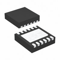
IC CONV BOOST LP 25MA 12-DFN

LT8415EDDB#TRPBF

Manufacturer Part Number
LT8415EDDB#TRPBF
Description
IC CONV BOOST LP 25MA 12-DFN
Manufacturer
Linear Technology
Type
Step-Up (Boost)r
Datasheet

Specifications of LT8415EDDB#TRPBF

Internal Switch(s)
Yes
Synchronous Rectifier
No
Number Of Outputs
1
Voltage - Output
2.5 ~ 40 V
Current - Output
25mA
Frequency - Switching
800kHz
Voltage - Input
2.5 ~ 16 V
Operating Temperature
-40°C ~ 125°C
Mounting Type
Surface Mount
Package / Case
12-DFN
Lead Free Status / RoHS Status
Lead free / RoHS Compliant
Power - Output
-

Available stocks

Company
Part Number
Manufacturer
Quantity
Price
Company:
Part Number:
LT8415EDDB#TRPBFLT8415EDDB
Manufacturer:
LT
Quantity:
10 000
Company:
Part Number:
LT8415EDDB#TRPBFLT8415EDDB#PBF/IDDB
Manufacturer:
SEC
Quantity:
57
Company:
Part Number:
LT8415EDDB#TRPBF
Manufacturer:
LT/凌特
Quantity:
20 000
n
n
n
n
n
n
n
n
n
n
n
n
n
n
APPLICATIONS
TYPICAL APPLICATION
FEATURES
n
n
n
n
*HIGHER VALUE CAPACITOR IS REQUIRED
WHEN THE V
**THIS CAPACITOR IS OPTIONAL
V
2.5V to 16V
IN
High Voltage Switches Built in (Dual half-bridge)
Ultralow Quiescent Current
Comparator Built into SHDN pin
Low Noise Control Scheme
Adjustable FB reference voltage
Wide Input Range: 2.5V to 16V
Wide Output Range: Up to 40V
Integrated Power NPN Switch (25mA Current Limit)
Integrated Schottky Diode
Integrated Output Disconnect
High Value (12.4M/0.4M) Feedback Resistor Integrated
Built in Soft Start (Optional Capacitor from V
Over Voltage Protection for CAP, V
OUT2 Pins
12-Pin 3mm × 2mm DFN package
Sensor Power
RF Mems Relay Power
Low Power Actuator Bias/Control
Liquid Lens Driver
10.5μA in Active Mode
0μA in Shutdown Mode
Drive External Capacitors to 34V/0V with the LT8415
IN
2.2μF
ENABLE
IS HIGHER THAN 8V
CHIP
LOGIC
LEVEL
100μH
V
IN 1
IN 2
SHDN
GND
SW
CC
LT8415
OUT 1
OUT 2
V
V
CAP
FBP
OUT
REF
137K
887K
22nF
OUT
0.1μF*
0.1μF**
, OUT1 and
34V/0V
V
OUT
8415 TA01
REF
= 34V
to GND)
34V/0V
DESCRIPTION
The LT
two integrated complementary MOSFET half-bridges
(N- and P-channel), integrated power switch, Schottky
diode and output disconnect circuitry. The N-channel and
P-channel MOSFETs in each half-bridge are synchronously
controlled by a single input pin, and never turn on at the
same time in typical applications.
The boost regulator controls power delivery by varying
both the peak inductor current and switch off-time. This
control scheme results in low output voltage ripple as well
as high effi ciency over a wide load range. The quiescent
current is a low 10.5μA, which is further reduced to 0μA
in shutdown. The internal disconnect circuitry allows the
output voltage to be blocked from the input during shut-
down. High value (12.4M/0.4M) resistors are integrated
on chip for output voltage detection, signifi cantly reducing
input referred quiescent current. The LT8415 also features a
comparator built into the SHDN pin, overvoltage protection
for the CAP, V
and comes in a tiny 12-pin 3mm × 2mm DFN package.
L, LT, LTC and LTM are registered trademarks of Linear Technology Corporation. Hot Swap
is a trademark of Linear Technology Corporation. All other trademarks are the property of their
respective owners. Protected by U.S. Patents including 5481178, 6580258, 6304066, 6127815,
6498466, 6611131.
OUT2 VOLTAGE
OUT1 VOLTAGE
IN2 VOLTAGE
IN1 VOLTAGE
®
2V/DIV
2V/DIV
8415 is an ultralow power boost converter with
20/DIV
20/DIV
Ultralow Power Boost
Response Driving External Capacitors
Half-Bridge Switches
C
C
OUT
Converter with Dual
OUT1
OUT2
, OUT1 and OUT2 pins, built in soft start
= 1nF
= 200pF
20μs/DIV
8415 TA02
LT8415
1
8415f

Related parts for LT8415EDDB#TRPBF

LT8415EDDB#TRPBF Summary of contents

Page 1

... DFN package. L, LT, LTC and LTM are registered trademarks of Linear Technology Corporation. Hot Swap is a trademark of Linear Technology Corporation. All other trademarks are the property of their respective owners. Protected by U.S. Patents including 5481178, 6580258, 6304066, 6127815, 6498466, 6611131 ...

Page 2

... ORDER INFORMATION LEAD FREE FINISH TAPE AND REEL LT8415EDDB#PBF LT8415EDDB#TRPBF LT8415IDDB#PBF LT8415IDDB#TRPBF Consult LTC Marketing for parts specifi ed with wider operating temperature ranges. *The temperature grade is identifi label on the shipping container. Consult LTC Marketing for information on non-standard lead based fi nish parts. ...

Page 3

ELECTRICAL CHARACTERISTICS temperature range, otherwise specifi cations are T PARAMETER PMOS Disconnect Current Limit PMOS Disconnect CAP OUT Internal Resistor Divider Ratio FBP pin Bias Current SHDN Minimum Input Voltage High SHDN Input Voltage High hysteresis SHDN ...

Page 4

LT8415 TYPICAL PERFORMANCE CHARACTERISTICS Output Voltage vs Temperature 3.6V 16V CC OUT LOAD = 0.5mA 0.75 FIGURE 4 CIRCUIT 0.5 0.25 0 – 0.25 – 0.5 – 0.75 –1 – TEMPERATURE ...

Page 5

TYPICAL PERFORMANCE CHARACTERISTICS SW Saturation Voltage vs Switch Current 300 250 200 150 100 SWITCH CURRENT (mA) 8415 G13 Output Disconnect PMOS current vs CAP to V Voltage Difference OUT ...

Page 6

LT8415 PIN FUNCTIONS SHDN (Pin 1): Shutdown Pin. This pin is used to enable/dis- able the chip. Drive below 0.3V to disable the chip. Drive above 1.4V to activate the chip. Do not fl oat this pin. V (Pin 2): ...

Page 7

TIMING DIAGRAM 2V IN1,IN2 VOLTAGE 0V 34V OUT1,OUT2 VOLTAGE 0V OPERATION Switching Regulator The LT8415 utilizes a variable peak current, variable off- time control scheme to provide high effi ciency over a wide output current range. The operation of the ...

Page 8

LT8415 APPLICATIONS INFORMATION Inductor Selection Several inductors that work well with the LT8415 are listed in Table 1. The tables are not complete, and there are many other manufacturers and devices that can be used. Consult each manufacturer for more ...

Page 9

APPLICATIONS INFORMATION Maximum Output Load Current The maximum output current of a particular LT8415 circuit is a function of several circuit variables. The following method can be helpful in predicting the maximum load current for a given circuit: Step 1: ...

Page 10

LT8415 APPLICATIONS INFORMATION If the application doesn’t require the output disconnect function, the CAP and V pin can be shorted, and higher OUT power converter effi ciency can be achieved. SHDN Pin Comparator and Hysteresis Current An internal comparator compares ...

Page 11

... ALL DIMENSIONS ARE IN MILLIMETERS Information furnished by Linear Technology Corporation is believed to be accurate and reliable. However, no responsibility is assumed for its use. Linear Technology Corporation makes no representa- tion that the interconnection of its circuits as described herein will not infringe on existing patent rights. OUT2 VOLTAGE ...

Page 12

... DFN OUT(MAX 40V 65μA, I < 1μA, DFN OUT(MAX 40V 1mA, I <1μA, MS8E OUT(MAX 40V 60μA, I < 1μA, DFN OUT(MAX 40V 8.5μA, I < 1μA, DFN OUT(MAX 0409 • PRINTED IN USA © LINEAR TECHNOLOGY CORPORATION 2009 < 1μA, 8415f ...

Related keywords