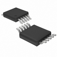
LTC3423EMS#TR Linear Technology, LTC3423EMS#TR Datasheet - Page 5

LTC3423EMS#TR
Manufacturer Part Number
LTC3423EMS#TR
Description
IC SYNC BOOST CONV MCRPWR 10MSOP
Manufacturer
Linear Technology
Type
Step-Up (Boost)r
Datasheet
1.LTC3423EMS.pdf
(12 pages)
Specifications of LTC3423EMS#TR
Internal Switch(s)
Yes
Synchronous Rectifier
Yes
Number Of Outputs
1
Voltage - Output
1.5 ~ 5.5 V
Current - Output
1A
Frequency - Switching
3MHz
Voltage - Input
0.5 ~ 5.5 V
Operating Temperature
-40°C ~ 85°C
Mounting Type
Surface Mount
Package / Case
10-MSOP, Micro10™, 10-uMAX, 10-uSOP
Power - Output
750mW
Lead Free Status / RoHS Status
Contains lead / RoHS non-compliant
Other names
LTC3423EMSTR
Available stocks
Company
Part Number
Manufacturer
Quantity
Price
TYPICAL PERFOR A CE CHARACTERISTICS
R
Frequency.
MODE/SYNC (Pin 2): Burst Mode Select and Oscillator
Synchronization.
V
PI FU CTIO S
IN
t
MODE/SYNC = High. Enable Burst Mode operation. The
inductor peak inductor current will be 400mA and
return to zero current on each cycle. During Burst Mode
operation the operation is variable frequency, providing
a significant efficiency improvement at light loads. It is
recommended the Burst Mode operation only be en-
tered once the part has started up.
MODE/SYNC = Low. Disable Burst Mode operation and
maintain low noise, constant frequency operation.
MODE/SYNC = External CLK. Synchronization of the
internal oscillator and Burst Mode operation disable. A
clock pulse width of 100ns to 2 s is required to
synchronize.
(Pin 1): Timing Resistor to Program the Oscillator
f
U
(Pin 3): Voltage Sense for Internal Circuitry.
OSC
U
3 10
•
R
t
10
1.00
0.95
0.90
0.85
0.80
0.75
0.70
0.65
0.60
1.10
1.05
Hz
–55
U
Shutdown Threshold
–15
W
TEMPERATURE ( C)
U
25
65
3423/24 G13
105
125
SW (Pin 4): Switch Pin. Connect inductor and optional
Schottky diode here. Minimize trace length to keep EMI
down.
GND (Pin 5): Signal and Power Ground for the IC.
V
from a higher voltage power converter. Requires an input
of 2.7V to 5.5V. A 2.2 F ceramic bypass capacitor is
recommended as close to the pins as possible.
V
FB (Pin 8): Feedback Pin. Connect resistor divider tap
here. The output voltage can be adjusted from 1.5V to
5.5V. The feedback reference voltage is typically 1.25V.
V
network is connected to this pin to compensate the loop.
See the section “Compensating the Feedback Loop” for
guidelines.
SHDN (Pin 10): Shutdown. Grounding this pin shuts down
the IC. Tie to >1V to enable (V
During shutdown the output voltage will hold up to V
minus a diode drop due to the body diode of the PMOS
synchronous switch. If the application requires a com-
plete disconnect during shutdown then refer to section
“Output Disconnect”.
DD
OUT
C
(Pin 9): Error Amp Output. A frequency compensation
(Pin 6): Power Source for the IC. Typically derived
(Pin 7): Output of the Synchronous Rectifier.
38
44
42
40
36
34
32
30
–55
Burst Mode Operation Current
–15
TEMPERATURE ( C)
25
LTC3423/LTC3424
65
DD
or digital gate output).
3423/24 G14
105
125
34234f
5
IN


