LTC3125EDCB#TRPBF Linear Technology, LTC3125EDCB#TRPBF Datasheet - Page 2
LTC3125EDCB#TRPBF
Manufacturer Part Number
LTC3125EDCB#TRPBF
Description
IC DC/DC CONV STP-UP 1.2A 8-DFN
Manufacturer
Linear Technology
Type
Step-Up (Boost)r
Datasheet
1.LTC3125EDCBTRMPBF.pdf
(18 pages)
Specifications of LTC3125EDCB#TRPBF
Internal Switch(s)
Yes
Synchronous Rectifier
Yes
Number Of Outputs
1
Voltage - Output
2 ~ 5.25 V
Current - Output
1.2A
Frequency - Switching
1.6MHz
Voltage - Input
1.8 ~ 5.5 V
Operating Temperature
-40°C ~ 85°C
Mounting Type
Surface Mount
Package / Case
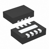
8-DFN
Lead Free Status / RoHS Status
Lead free / RoHS Compliant
Power - Output
-
Available stocks
Company
Part Number
Manufacturer
Quantity
Price


ABSOLUTE MAXIMUM RATINGS
LTC3125
(Note 1)
V
SW Voltage .................................................. –0.3V to 6V
SW Voltage < 100ns .................................... –0.3V to 7V
All Other Pins ............................................... –0.3V to 6V
Operating Junction Temperature Range
(Notes 2, 5) ............................................ –40°C to 125°C
Junction Temperature ........................................... 125°C
Storage Temperature Range ................... –65°C to 125°C
ORDER INFORMATION
LEAD FREE FINISH
LTC3125EDCB#PBF
Consult LTC Marketing for parts specifi ed with wider operating temperature ranges.
Consult LTC Marketing for information on non-standard lead based fi nish parts.
For more information on lead free part marking, go to:
For more information on tape and reel specifi cations, go to:
PARAMETER
Input Voltage Range
Minimum Start-Up Voltage
Output Voltage Adjust Range
Feedback Voltage
Feedback Input Current
Quiescent Current—Shutdown
Quiescent Current —Active
Quiescent Current—Burst
N-Channel MOSFET Switch Leakage
P-Channel MOSFET Switch Leakage
N-Channel MOSFET Switch On-Resistance
P-Channel MOSFET Switch On-Resistance
N-Channel MOSFET Current Limit
Current Limit Delay to Output
Average Input Current Limit
ELECTRICAL CHARACTERISTICS
2
junction temperature range, otherwise specifi cations are at T
IN
, V
OUT
Voltage ......................................... –0.3V to 6V
TAPE AND REEL
LTC3125EDCB#TRPBF
CONDITIONS
V
Measured on V
V
Nonswitching
V
V
V
V
(Note 3)
R
R
SHDN
IN
SW
SW
OUT
OUT
PROG
PROG
http://www.linear.com/leadfree/
= V
= 5V, V
= 5V, V
= 3.3V
= 3.3V
PART MARKING
LDGY
= 0V, Not Including Switch Leakage, V
= 44.2k
= 44.2k, (Note 4)
OUT
http://www.linear.com/tapeandreel/
= 3.3V, Measured on V
IN
OUT
= 5V
OUT
= 0V, V
The
, Nonswitching
A
= 25°C. V
l
IN
denotes the specifi cations which apply over the full operating
= 5V
PIN CONFIGURATION
IN
IN
PACKAGE DESCRIPTION
8-Lead (2mm × 3mm) Plastic DFN
= 3.3V, V
, FB ≥ 1.230V,
EXPOSED PAD (PIN 9) IS GND, MUST BE SOLDERED TO PCB
OUT
OUT
PROG
= 0V
GND
= 4.5V unless otherwise noted (Note 2).
V
FB
8-LEAD (2mm 3mm) PLASTIC DFN
T
IN
JMAX
1
2
3
4
= 125°C, θ
l
l
l
l
l
DCB PACKAGE
TOP VIEW
JA
1.176
MIN
475
465
9
1.8
1.2
= 64°C/W (NOTE 6)
2
1.200
0.125
0.200
0.01
TYP
300
500
500
1.6
0.1
0.1
1.8
8
7
6
5
TEMPERATURE RANGE
–40°C to 125°C
15
60
1
SW
V
SHDN
CS
OUT
1.229
MAX
5.25
500
525
535
5.5
1.8
50
25
10
20
1
UNITS
3125fa
mA
mA
nA
μA
μA
μA
μA
μA
ns
Ω
Ω
V
V
V
V
A
Related parts for LTC3125EDCB#TRPBF
Image
Part Number
Description
Manufacturer
Datasheet
Request
R

Part Number:
Description:
1.2A Synchronous Step-Up DC/DC Converter
Manufacturer:
Linear Technology
Datasheet:
Part Number:
Description:
CD ROM LINEARVIEW DATASHEETS
Manufacturer:
Linear Technology

Part Number:
Description:
Standalone Linear Li-Ion Battery Charger with Thermal Regulation in ThinSOT
Manufacturer:
Linear Technology Corporation
Datasheet:
Part Number:
Description:
Low noise, high frequency, 8th order linear phase lowpass filter
Manufacturer:
Linear Technology Corporation
Datasheet:
Part Number:
Description:
Manufacturer:
Linear Technology Corporation
Datasheet:
Part Number:
Description:
Manufacturer:
Linear Technology Corporation
Datasheet:
Part Number:
Description:
Manufacturer:
Linear Technology Corporation
Datasheet:
Part Number:
Description:
Manufacturer:
Linear Technology Corporation
Datasheet:
Part Number:
Description:
Manufacturer:
Linear Technology Corporation
Datasheet:
Part Number:
Description:
Manufacturer:
Linear Technology Corporation
Datasheet:
Part Number:
Description:
Manufacturer:
Linear Technology Corporation
Datasheet:
Part Number:
Description:
Dual and Quad, JFET Input Precision High Speed Op Amps
Manufacturer:
Linear Technology Corporation
Datasheet:
Part Number:
Description:
Manufacturer:
Linear Technology Corporation
Datasheet:
Part Number:
Description:
1, 2, 6 and 8 Channel, 10-Bit Serial I/O Data Acquisition Systems
Manufacturer:
Linear Technology Corporation
Datasheet:
Part Number:
Description:
Manufacturer:
Linear Technology Corporation
Datasheet: