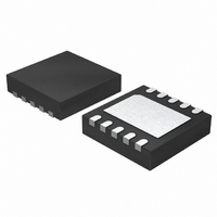
LT3757EDD#TRPBF Linear Technology, LT3757EDD#TRPBF Datasheet - Page 22

LT3757EDD#TRPBF
Manufacturer Part Number
LT3757EDD#TRPBF
Description
IC CTRLR DC/DC ADJ 10-DFN
Manufacturer
Linear Technology
Type
Step-Up (Boost), Inverting, Flyback, Sepicr
Datasheet
1.LT3757EDDPBF.pdf
(36 pages)
Specifications of LT3757EDD#TRPBF
Internal Switch(s)
No
Synchronous Rectifier
No
Number Of Outputs
1
Frequency - Switching
100kHz ~ 1MHz
Voltage - Input
2.9 ~ 40 V
Operating Temperature
-40°C ~ 125°C
Mounting Type
Surface Mount
Package / Case
10-DFN
Lead Free Status / RoHS Status
Lead free / RoHS Compliant
Current - Output
-
Voltage - Output
-
Power - Output
-
Available stocks
Company
Part Number
Manufacturer
Quantity
Price
LT3757
applicaTions inForMaTion
that, in the SEPIC converter, the inductor L1 is in series
with the input, and the ripple current flowing through the
input capacitor is continuous.
SEPIC Converter: Switch Duty Cycle and Frequency
For a SEPIC converter operating in CCM, the duty cycle
of the main switch can be calculated based on the output
voltage (V
forward voltage (V
The maximum duty cycle (D
has the minimum input voltage:
SEPIC Converter: Inductor and Sense Resistor Selection
As shown in Figure 1, the SEPIC converter contains two
inductors: L1 and L2. L1 and L2 can be independent, but
can also be wound on the same core, since identical volt-
ages are applied to L1 and L2 throughout the switching
cycle.
For the SEPIC topology, the current through L1 is the
converter input current. Based on the fact that, ideally, the
output power is equal to the input power, the maximum
average inductor currents of L1 and L2 are:
D
I
I
L MAX
L MAX
MAX
1
2
(
(
=
)
) )
OUT
=
V
=I
IN MIN
I
IN MAX
O MAX
), the input voltage (V
(
(
(
V
OUT
)
D
+
).
)
)
=
V
+
OUT
I
V
O MAX
(
D
MAX
+
V
)
) occurs when the converter
D
•
Figure 9. The Switch Current Waveform of the SEPIC Converter
1
I
SW
−
D
MAX
D
MAX
IN
) and the diode
I
SW(MAX)
DT
S
T
S
I
SW =
In a SEPIC converter, the switch current is equal to I
I
average switch current is defined as:
and the peak switch current is:
The constant c in the preceding equations represents the
percentage peak-to-peak ripple current in the switch, rela-
tive to I
ripple current ∆I
∆I
The inductor ripple currents ∆I
∆I
The inductor ripple current has a direct effect on the
choice of the inductor value. Choosing smaller values of
∆I
loop gain (the converter will approach voltage mode).
Accepting larger values of ∆I
ductances, but results in higher input current ripple and
greater core losses. It is recommended that c falls in the
range of 0.2 to 0.4.
L2
I
SW(MAX)
L
when the power switch is on, therefore, the maximum
I
I
requires large inductances and reduces the current
SW MAX
SW PEAK
SW
L1
(
(
= ∆I
SW(MAX)
= c • I
)
)
L2
=
=
I
= 0.5 • ∆I
SW(MAX)
L MAX
, as shown in Figure 9. Then, the switch
1
1
SW
(
+
can be calculated by:
3757 F08
c
2
)
t
+
•
I
I
SW
O MAX
L MAX
2
(
(
L
allows the use of low in-
L1
)
)
•
and ∆I
=
1
I
−
O MAX
D
(
1
MAX
L2
)
•
are identical:
1
−
D
1
MAX
3757fb
L1
+


