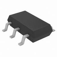
LTC3459ES6#TRPBF Linear Technology, LTC3459ES6#TRPBF Datasheet - Page 6

LTC3459ES6#TRPBF
Manufacturer Part Number
LTC3459ES6#TRPBF
Description
IC BOOST SYNC ADJ SOT23-6
Manufacturer
Linear Technology
Type
Step-Up (Boost)r
Datasheet
1.LTC3459ES6TR.pdf
(12 pages)
Specifications of LTC3459ES6#TRPBF
Internal Switch(s)
Yes
Synchronous Rectifier
Yes
Number Of Outputs
1
Voltage - Output
2.5 ~ 10 V
Voltage - Input
1.5 ~ 5.5 V
Operating Temperature
-40°C ~ 85°C
Mounting Type
Surface Mount
Package / Case
TSOT-23-6, TSOT-6
Primary Input Voltage
5.5V
No. Of Outputs
1
Output Voltage
10V
Output Current
75mA
No. Of Pins
6
Operating Temperature Range
-40°C To +85°C
Msl
MSL 1 - Unlimited
Rohs Compliant
Yes
Lead Free Status / RoHS Status
Lead free / RoHS Compliant
Current - Output
-
Power - Output
-
Frequency - Switching
-
Available stocks
Company
Part Number
Manufacturer
Quantity
Price
PIN FUNCTIONS
LTC3459
V
a low ESR, ESL ceramic capacitor of at least 1μF .
V
the Boost Regulator. Bypass V
ceramic capacitor between 2.2μF and 10μF . V
increases with smaller capacitors.
SHDN (Pin 3/Pin 1/Pin 4): Master Shutdown Input. Driving
SHDN low disables all IC functions and reduces quiescent
current from the battery to less than 1μA. This pin must
be pulled above 1V to enable the IC.
FB (Pin 4/Pin 3/Pin 3): Input to the Burst Mode Comparator.
An external resistor divider connected between V
GND and this pin sets the output voltage to:
BLOCK DIAGRAM
6
IN
OUT
V
(Pin 1/Pin 6/Pin 6): Input Supply Pin. Bypass V
OUT
(Pin 2/Pin 2/Pin 5): Regulated Output Voltage of
P/~N
= 1.22(1 + R1/R2)
P-DRIVE
I
ZO
SDB
Q
QB
S
RD
V
OUT
RD
QB
S
Q
SD
N-DRIVE
V
TIMER
SELECT
t
V
OFF
CC
(DC/DCB/S6 Packages)
THERMAL
OUT
Q
QB
V
CC
SD
DETECT
with a low ESR, ESL
SD
I
PEAK
R
I
t
PEAK
OFF
V
OUT
BEST
DELAY
N-DRIVE
SLEEP
IN
ripple
with
OUT
I
ZO
,
SW
GND
OFF ON
GND (Pin 5/Pin 5/Pin 2): Signal and Power Ground. Provide
a short, direct PCB path between GND and the (–) side of
the fi lter capacitors on V
SW (Pin 6/Pin 4/Pin 1): Switch Pin. Connect a 15μH to
33μH inductor between SW and V
as short and wide as possible to reduce EMI and voltage
overshoot. If the inductor current falls to zero, the internal
P-channel MOSFET synchronous rectifi er is turned off to
prevent reverse charging of the inductor.
Exposed Pad (Pin 7/Pin 7, DC and DCB Packages Only):
Ground. The Exposed Pad must be soldered to PCB.
HYSTCOMP
DETECT
I
ZERO
P-DRIVE
V
BEST
SHDN
SW1
V
REFOK
SELECT
–
+
REFERENCE
IN
and V
V
CC
–
+
IN
OUT
. Keep PCB trace lengths
.
SD
SDB
V
OUT
V
FB
3459 BD
IN
R1
R2
3459fc


