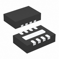
LT8410EDC-1#TRPBF Linear Technology, LT8410EDC-1#TRPBF Datasheet

LT8410EDC-1#TRPBF
Specifications of LT8410EDC-1#TRPBF
Available stocks
Related parts for LT8410EDC-1#TRPBF
LT8410EDC-1#TRPBF Summary of contents
Page 1
... SHDN pin, overvoltage protection for the CAP and V pins, built in soft-start and comes in a tiny 8-pin 2mm × 2mm DFN package. REF L, LT, LTC, LTM, Linear Technology and the Linear logo are registered trademarks of Linear Pins Technology Corporation. Hot Swap is a trademark of Linear Technology Corporation. All other OUT trademarks are the property of their respective owners ...
Page 2
... LT8410EDC#PBF LT8410EDC#TRPBF LT8410IDC#PBF LT8410IDC#TRPBF LT8410EDC-1#PBF LT8410EDC-1#TRPBF LT8410IDC-1#PBF LT8410IDC-1#TRPBF Consult LTC Marketing for parts specified with wider operating temperature ranges. *The temperature grade is identified by a label on the shipping container. Consult LTC Marketing for information on non-standard lead based finish parts. For more information on lead free part marking, go to: ...
Page 3
ELECTRICAL CHARACTERISTICS temperature range, otherwise specifications are at T PARAMETER Switch V CESAT Switch Leakage Current Schottky Forward Voltage Schottky Reverse Leakage PMOS Disconnect Current Limit PMOS Disconnect V – V CAP OUT V Resistor Divider Ratio OUT FBP Pin ...
Page 4
LT8410/LT8410-1 TYPICAL PERFORMANCE CHARACTERISTICS Output Voltage vs Temperature 1. 3.6V 16V CC OUT 0.75 LOAD = 0.5mA FIGURE 4 CIRCUIT 0.50 0.25 0 – 0.25 – 0.50 – 0.75 –1.00 – TEMPERATURE ...
Page 5
TYPICAL PERFORMANCE CHARACTERISTICS LT8410 Switching Waveform at No Load V VOLTAGE OUT 2mV/DIV AC COUPLED SW VOLTAGE 10V/DIV INDUCTOR CURRENT 10mA/DIV V = 3.6V 50µs/DIV 16V OUT LT8410 Switching Waveform at 3mA Load V VOLTAGE OUT 10mV/DIV ...
Page 6
LT8410/LT8410-1 TYPICAL PERFORMANCE CHARACTERISTICS Output Disconnect PMOS Current vs CAP to V Voltage Difference OUT 16V CAP LT8410 LT8410 CAP TO V VOLTAGE DIFFERENCE (V) OUT LT8410 Start-Up Waveforms ...
Page 7
PIN FUNCTIONS SHDN (Pin 1): Shutdown Pin. This pin is used to enable/ disable the chip. Drive below 0.3V to disable the chip. Drive above 1.45V to activate the chip. Do not float this pin. V (Pin 2): Input Supply ...
Page 8
LT8410/LT8410-1 OPERATION The LT8410 series utilizes a variable peak current, variable off-time control scheme to provide high efficiency over a wide output current range. The operation of the part can be better understood by referring to the Block Diagram. The ...
Page 9
APPLICATIONS INFORMATION or 0805 size capacitor will be adequate. A 0.1μF to 1μF capacitor placed on the CAP node is recommended to filter the inductor current, while a 0.1μF to 1μF capacitor placed on the V node will give excellent ...
Page 10
LT8410/LT8410-1 APPLICATIONS INFORMATION Step 4. Calculate the nominal output current: I • V • 0.7 IN(AVG OUT(NOM) V OUT Step 5. Derate output current: • 0 OUT OUT(NOM) For low output voltages the output ...
Page 11
APPLICATIONS INFORMATION Board Layout Considerations As with all switching regulators, careful attention must be paid to the PCB layout and component placement. To maximize efficiency, switch rise and fall times are made as short as possible. To prevent electromagnetic interference ...
Page 12
LT8410/LT8410-1 TYPICAL APPLICATIONS 100µH 2.5V to 16V C1 2.2µF SW CAP OUT LT8410 V REF TURN ON/OFF SHDN GND FBP C1: 2.2 F, 16V, X5R, 0603 C2: 0.1 F, 25V, X5R, 0603 C3: 0.1 ...
Page 13
TYPICAL APPLICATIONS 34V Output Converter with Wide Input Voltage 150µH 2.5V to 16V C1 2.2µF SW CAP OUT LT8410 V REF TURN ON/OFF SHDN GND FBP C1: 2.2 F, 16V, X5R, 0603 C2: 0.1 ...
Page 14
LT8410/LT8410-1 PACKAGE DESCRIPTION 2.55 ±0.05 0.64 ±0.05 1.15 ±0.05 (2 SIDES) RECOMMENDED SOLDER PAD PITCH AND DIMENSIONS APPLY SOLDER MASK TO AREAS THAT ARE NOT SOLDERED PIN 1 BAR TOP MARK (SEE NOTE 6) 0.200 REF 14 DC Package 8-Lead ...
Page 15
... Revised Note 2 in Electrical Characteristics Information furnished by Linear Technology Corporation is believed to be accurate and reliable. However, no responsibility is assumed for its use. Linear Technology Corporation makes no representa- tion that the interconnection of its circuits as described herein will not infringe on existing patent rights. LT8410/LT8410-1 ...
Page 16
... OUT(MAX 34V 25µA, I < 1µA, OUT(MAX ±40V 2.5mA, I < 1µA, OUT(MAX 36V 100µA, I < 1µA, OUT(MAX 40V 65µA, I < 1µA, OUT(MAX 40V 60µA, I < 1µA, OUT(MAX 0211 REV B • PRINTED IN USA LINEAR TECHNOLOGY CORPORA TION 2008 84101fb ...


