LT3467AEDDB#TRMPBF Linear Technology, LT3467AEDDB#TRMPBF Datasheet
LT3467AEDDB#TRMPBF
Specifications of LT3467AEDDB#TRMPBF
Available stocks


Related parts for LT3467AEDDB#TRMPBF


LT3467AEDDB#TRMPBF Summary of contents
Page 1
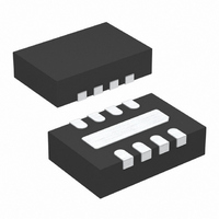
... LT3467A are available in a low profi le (1mm) 6-lead SOT-23 package and tiny 3mm × 2mm DFN package. L, LT, LTC, LTM, Linear Technology and the Linear logo are registered trademarks of Linear Technology Corporation. ThinSOT is a trademark of Linear Technology Corporation. All other trademarks are the property of their respective owners ...
Page 2
LT3467/LT3467A ABSOLUTE MAXIMUM RATINGS V Voltage ................................................................16V IN SW Voltage ................................................ –0.4V to 42V FB Voltage ................................................................2.5V Current Into FB Pin .............................................. ±1mA SHDN Voltage ......................................................... 16V Maximum Junction Temperature ......................... 125°C PIN CONFIGURATION TOP VIEW GND ...
Page 3
ELECTRICAL CHARACTERISTICS temperature range, otherwise specifi cations are at T the LT3467 and LT3467A unless otherwise noted. PARAMETER CONDITIONS Minimum Operating Voltage Maximum Operating Voltage Feedback Voltage FB Pin Bias Current (Note 3) Quiescent Current V SHDN Quiescent Current in ...
Page 4
LT3467/LT3467A TYPICAL PERFORMANCE CHARACTERISTICS Quiescent Current vs Temperature 1.6 1.4 1.2 1.0 0.8 0.6 0.4 0.2 0 –40 –25 – 110 TEMPERATURE (°C) 3467 G01 Current Limit vs Duty Cycle 2 ...
Page 5
PIN FUNCTIONS (DFN/TSOT) FB (Pin 1/Pin 3): Feedback Pin. Reference voltage is 1.255V. Connect resistive divider tap here. Minimize trace area at FB. Set V = 1.255V(1 + R1/R2). OUT GND (Pins 2, 5, 9/Pin 2): Ground. Tie directly to ...
Page 6
LT3467/LT3467A OPERATION The LT3467 uses a constant frequency, current-mode con- trol scheme to provide excellent line and load regulation. Refer to the Block Diagram. At the start of each oscillator cycle, the SR latch is set which turns on the ...
Page 7
APPLICATIONS INFORMATION V IN 2.6V TO 4.2V Figure 2. Single Li-Ion Cell to 5V Boost Converter (Same as 1st Page Application) Table 1. Inductor Manufacturers Sumida (847) 956-0666 TDK (847) 803-6100 Murata (714) 852-2001 FDK (408) 432-8331 Soft-Start The soft-start ...
Page 8
LT3467/LT3467A APPLICATIONS INFORMATION Capacitor Selection Low ESR (equivalent series resistance) capacitors should be used at the output to minimize the output ripple voltage. Multi-layer ceramic capacitors are an excellent choice, as they have extremely low ESR and are available in ...
Page 9
APPLICATIONS INFORMATION LOAD CURRENT 100mA/DIV AC COUPLED V OUT 200mV/DIV AC COUPLED I L1 5A/DIV AC COUPLED 20μs/DIV Figure 3. Transient Response of Figure 8’s Step-Up Converter without Phase Lead Capacitor LOAD CURRENT 100mA/DIV AC COUPLED V OUT 200mV/DIV AC ...
Page 10
LT3467/LT3467A APPLICATIONS INFORMATION Compensation—Theory Like all other current mode switching regulators, the LT3467/LT3467A needs to be compensated for stable and effi cient operation. Two feedback loops are used in the LT3467/LT3467A: a fast current loop which does not require compensation, ...
Page 11
APPLICATIONS INFORMATION Using the circuit of Figure example, the following table shows the parameters used to generate the Bode plot shown in Figure –10 –20 –30 GAIN –40 PHASE –50 ...
Page 12
LT3467/LT3467A TYPICAL APPLICATIONS 4V TO 6.5V C1 2.2μF 4-CELL BATTERY 0.047μF C1, C3: X5R or X7R, 10V C2: X5R or X7R, 6. 2.2μF OFF ON 0.047μF C1: X5R or X7R, 6. C5: X5R ...
Page 13
TYPICAL APPLICATIONS 9V, 18V, –9V Triple Output TFT-LCD Bias Supply with Soft-Start D1 L1 4.7μ 3.3V C1 2.2μ SHDN SHDN LT3467 SS FB 3.3V GND 0V C7 0.1μF C1: X5R OR X7R, 6.3V C2,C3, ...
Page 14
LT3467/LT3467A TYPICAL APPLICATIONS Single Li-Ion Cell to 5V Boost Converter L1 0.9μ 2. 4.7μF SHDN OFF ON LT3467A GND 0.047μF C1, C2: X5R OR X7R, 6.3V D1: PHILIPS PMEG ...
Page 15
PACKAGE DESCRIPTION 0.61 0.05 (2 SIDES) 0.70 0.05 2.55 0.05 1.15 0.05 0.25 0.05 0.50 BSC 2.20 0.05 (2 SIDES) RECOMMENDED SOLDER PAD PITCH AND DIMENSIONS NOTE: 1. DRAWING CONFORMS TO VERSION (WECD-1) IN JEDEC PACKAGE OUTLINE M0-229 2. DRAWING ...
Page 16
LT3467/LT3467A PACKAGE DESCRIPTION 0.62 0.95 MAX REF 3.85 MAX 2.62 REF RECOMMENDED SOLDER PAD LAYOUT PER IPC CALCULATOR 0.20 BSC DATUM ‘A’ 0.30 – 0.50 REF NOTE: 1. DIMENSIONS ARE IN MILLIMETERS 2. DRAWING NOT TO SCALE 3. DIMENSIONS ARE ...
Page 17
... Updated Note 2 in Absolute Maximum Ratings and Electrical Characteristics Information furnished by Linear Technology Corporation is believed to be accurate and reliable. However, no responsibility is assumed for its use. Linear Technology Corporation makes no representa- tion that the interconnection of its circuits as described herein will not infringe on existing patent rights. ...
Page 18
... LTC3402 3MHz, Synchronous Step-Up DC/DC Converter SW LT3464 85mA (I ), High Effi ciency Step-Up DC/DC Converter with SW Integrated Schottky and PNP Disconnect trademark of Linear Technology Corporation. SENSE 18 Linear Technology Corporation 1630 McCarthy Blvd., Milpitas, CA 95035-7417 (408) 432-1900 FAX: (408) 434-0507 ● V OUT 12V ...