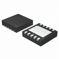
LT3495BEDDB-1#TRPBF Linear Technology, LT3495BEDDB-1#TRPBF Datasheet

LT3495BEDDB-1#TRPBF
Specifications of LT3495BEDDB-1#TRPBF
Available stocks
Related parts for LT3495BEDDB-1#TRPBF
LT3495BEDDB-1#TRPBF Summary of contents
Page 1
... APPLICATIONS n OLED Power n Low Noise Power n MP3 Player L, LT, LTC and LTM are registered trademarks of Linear Technology Corporation. All other trademarks are the property of their respective owners. *Patent pending. TYPICAL APPLICATION OLED Power Supply from One Li-Ion Cell 10μH ONE Li-Ion CELL 4.7μ ...
Page 2
... LT3495EDDB-1#TRPBF LT3495BEDDB#PBF LT3495BEDDB#TRPBF LT3495BEDDB-1#PBF LT3495BEDDB-1#TRPBF Consult LTC Marketing for parts specifi ed with wider operating temperature ranges. Consult LTC Marketing for information on non-standard lead based fi nish parts. For more information on lead free part marking, go to: For more information on tape and reel specifi cations, go to: ELECTRICAL CHARACTERISTICS temperature range, otherwise specifi ...
Page 3
ELECTRICAL CHARACTERISTICS temperature range, otherwise specifi cations are at T PARAMETER Switch Current Limit Switch V CESAT Switch Leakage Current PMOS Disconnect Current Limit PMOS Disconnect V – V CAP OUT V – V Clamp Voltage CAP OUT SHDN Input ...
Page 4
LT3495/LT3495B/ LT3495-1/LT3495B-1 TYPICAL PERFORMANCE CHARACTERISTICS Output Voltage vs Temperature 1. 3. 16V 0.75 OUT LOAD = 5mA FIGURE 7 CIRCUIT 0.50 0.25 0.00 –0.25 –0.50 –0.75 –1.00 – TEMPERATURE (°C) 3495 G04 ...
Page 5
TYPICAL PERFORMANCE CHARACTERISTICS LT3495 Switching Waveform at No Load V VOLTAGE OUT 10mV/DIV AC COUPLED SW VOLTAGE 10V/DIV INDUCTOR CURRENT 100mA/DIV 10μs/DIV 16V OUT LT3495 Switching Waveform at 80mA V VOLTAGE OUT 50mV/DIV AC ...
Page 6
LT3495/LT3495B/ LT3495-1/LT3495B-1 TYPICAL PERFORMANCE CHARACTERISTICS Line Regulation 0.30 0.25 0.20 0.15 0.10 0. VOLTAGE (V) CC SHDN VOLTAGE INDUCTOR CURRENT CAP VOLTAGE V OUT LT3495 Transient Response 20mA → 60mA → 20mA LOAD PULSE V ...
Page 7
PIN FUNCTIONS GND (Pins 1, 2): Ground. Tie directly to local ground plane. V (Pin 3): Input Supply Pin. Must be locally by- CC passed. CTRL (Pin 4): Dimming Pin. If not used, tie CTRL to 1.5V or higher. If ...
Page 8
LT3495/LT3495B/ LT3495-1/LT3495B-1 OPERATION The LT3495 series utilizes a variable peak current, variable off-time control scheme to provide high effi ciency over a wide range of output current. The operation of the part can be better understood by referring to the ...
Page 9
APPLICATIONS INFORMATION Inductor Selection Several inductors that work well with the LT3495/LT3495B are listed in Table 2 and those for the LT3495-1/LT3495B-1 are listed in Table 3. These tables are not complete, and there are many other manufacturers and devices ...
Page 10
LT3495/LT3495B/ LT3495-1/LT3495B-1 APPLICATIONS INFORMATION Setting Output Voltage and the Auxiliary Reference Input The LT3495 series is equipped with both an internal 1.235V reference and an auxiliary reference input. This allows the user to select between using the built-in refer- ence ...
Page 11
APPLICATIONS INFORMATION Maximum Output Load Current The maximum output current of a particular LT3495 series circuit is a function of several circuit variables. The fol- lowing method can be helpful in predicting the maximum load current for a given circuit: ...
Page 12
LT3495/LT3495B/ LT3495-1/LT3495B-1 APPLICATIONS INFORMATION can be set by the value of R and C CTRL expression can be used to design the soft-start time • C •In START UP CTRL CTRL is the voltage at SHDN pin ...
Page 13
TYPICAL APPLICATIONS L1 D1 10μH ONE Li-Ion CELL C1 4.7μF SW CAP OUT LT3495 SHDN TURN ON/OFF FB V DIMMING CTRL GND OUT C1: 4.7μF , 6.3V, X5R, 0603 C2: 2.2μF , 25V, X5R, 0805 C3: 1μF ...
Page 14
LT3495/LT3495B/ LT3495-1/LT3495B-1 TYPICAL APPLICATIONS One Li-Ion Cell Input Boost Converter with the LT3495-1/LT3495B 10μH ONE LI-ION CELL C1 2.2μF SW CAP OUT LT3495B-1/ LT3495-1 SHDN TURN ON/OFF FB V DIMMING CTRL GND OUT C1: 2.2μF ...
Page 15
... SHADED AREA IS ONLY A REFERENCE FOR PIN 1 LOCATION ON THE TOP AND BOTTOM OF PACKAGE Information furnished by Linear Technology Corporation is believed to be accurate and reliable. However, no responsibility is assumed for its use. Linear Technology Corporation makes no representa- tion that the interconnection of its circuits as described herein will not infringe on existing patent rights. ...
Page 16
... I < 1μA, OUT(MAX 40V 1.2mA, I < 1μA, OUT(MAX ±40V 2.5mA, I < 1μA, OUT(MAX 36V 100μA, I < 1μA, OUT(MAX 40V 65μA, I < 1μA, OUT(MAX 40V 1mA, I < 1μA, OUT(MAX 0209 REV A • PRINTED IN USA © LINEAR TECHNOLOGY CORPORATION 2008 3495b1b1fa ...


