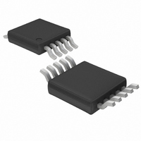
LT1618EMS Linear Technology, LT1618EMS Datasheet - Page 4

LT1618EMS
Manufacturer Part Number
LT1618EMS
Description
IC DC/DC CONV STEP-UP 10-MSOP
Manufacturer
Linear Technology
Type
Step-Up (Boost)r
Datasheet
1.LT1618EMSPBF.pdf
(16 pages)
Specifications of LT1618EMS
Internal Switch(s)
Yes
Synchronous Rectifier
No
Number Of Outputs
1
Voltage - Output
1.26 ~ 36 V
Current - Output
1.5A
Frequency - Switching
1.4MHz
Voltage - Input
1.6 ~ 18 V
Operating Temperature
-40°C ~ 85°C
Mounting Type
Surface Mount
Package / Case
10-MSOP, Micro10™, 10-uMAX, 10-uSOP
Lead Free Status / RoHS Status
Contains lead / RoHS non-compliant
Power - Output
-
Available stocks
Company
Part Number
Manufacturer
Quantity
Price
Company:
Part Number:
LT1618EMS
Manufacturer:
LT
Quantity:
10 000
Part Number:
LT1618EMS
Manufacturer:
LINEAR/凌特
Quantity:
20 000
Part Number:
LT1618EMS#PBF
Manufacturer:
LT/凌特
Quantity:
20 000
Part Number:
LT1618EMS8
Manufacturer:
LT/凌特
Quantity:
20 000
LT1618
PIN
FB (Pin 1/Pin 1): Feedback Pin. Set the output voltage by
selecting values for R1 and R2 (see Figure 1):
ISN (Pin 2/Pin 2): Current Sense (–) Pin. The inverting
input to the current sense amplifier.
ISP (Pin 3/Pin 3): Current Sense (+) Pin. The noninverting
input to the current sense amplifier.
I
applied to this pin will reduce the current sense voltage. If
this adjustment is not needed, tie this pin to ground.
GND (Pin 5/Pin 5): Ground Pin. Tie this pin directly to local
ground plane.
NC (Pin 6/NA): No Connection for MS Package.
TYPICAL PERFOR A CE CHARACTERISTICS
4
ADJ
R
1.8
1.7
1.6
1.5
1.4
1.3
1.2
1.1
1.0
U
1
(Pin 4/Pin 4): Current Sense Adjust Pin. A DC voltage
– 50
=
Switching Frequency
FUNCTIONS
R
– 25
2
⎛
⎜
⎝
U
1 263
V
.
OUT
0
TEMPERATURE (°C)
V
IN
V
25
= 18V
–
U
1
⎞
⎟
⎠
50
V
IN
75
= 1.6V
(MS/DD)
W
100
1618 G07
U
125
1.6
1.4
1.2
1.0
0.8
0.6
0.4
0.2
0
0
Frequency Foldback
T
J
= 25°C
0.2
FEEDBACK PIN VOLTAGE (V)
0.4
0.6
SW (NA/Pin 6): Switch Pin for DD Package. Connect this
pin to Pin 7.
SW (Pin 7/Pin 7): Switch Pin. This is the collector of the
internal NPN power switch. Minimize the metal trace area
connected to this pin to minimize EMI.
V
a capacitor to ground as close to the device as possible.
SHDN (Pin 9/Pin 9): Shutdown Pin. Tie this pin higher
than 1V to turn on the LT1618; tie below 0.3V to turn it off.
V
Connect a series RC from this pin to ground. Typical values
are 2kΩ and 10nF.
Exposed Pad (NA/Pin 11): The Exposed Pad on the DD
package is GND and must be soldered to the PCB GND for
optimum thermal performance.
IN
C
(Pin 10/Pin 10): Compensation Pin for Error Amplifier.
(Pin 8/Pin 8): Input Supply Pin. Bypass this pin with
0.8
1.0
1618 G08
1.2
50
45
40
35
30
25
20
15
10
5
0
SHDN Pin Current
0
SHUTDOWN PIN VOLTAGE (V)
5
T
J
= – 50°C
10
T
J
= 25°C
T
J
= 125°C
sn1618 1618fas
15
1618 G09
20


