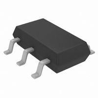
LTC1928ES6-5#TRM Linear Technology, LTC1928ES6-5#TRM Datasheet - Page 7

LTC1928ES6-5#TRM
Manufacturer Part Number
LTC1928ES6-5#TRM
Description
IC CHARGE PUMP DOUBLR LN SOT23-6
Manufacturer
Linear Technology
Type
Switched Capacitor (Charge Pump), Doublerr
Datasheet
1.LTC1928ES6-5TRM.pdf
(8 pages)
Specifications of LTC1928ES6-5#TRM
Internal Switch(s)
Yes
Synchronous Rectifier
No
Number Of Outputs
1
Voltage - Output
5V
Current - Output
30mA
Frequency - Switching
550kHz
Voltage - Input
2.7 ~ 4.4 V
Operating Temperature
-40°C ~ 85°C
Mounting Type
Surface Mount
Package / Case
TSOT-23-6, TSOT-6
Lead Free Status / RoHS Status
Contains lead / RoHS non-compliant
Power - Output
-
Other names
LTC1928ES6-5
LTC1928ES6-5
LTC1928ES65
Q1143368B
LTC1928ES6-5
LTC1928ES65
Q1143368B
Available stocks
Company
Part Number
Manufacturer
Quantity
Price
APPLICATIONS
Power-On Reset
Upon initial power-up, a power-on reset circuit ensures
that the internal functions are correctly initialized. Once
V
enable the part as long as the CN/SHDN pin is not pulled
low.
Thermal Considerations
The power handling capability of the device will be limited
by the maximum rated junction temperature (125 C). The
device dissipation P
device dissipates the majority of its heat through its pins,
especially GND (Pin 2). Thermal resistance to ambient can
be optimized by connecting GND to a large copper region
on the PCB, which serves as a heat sink. Applications that
operate the LTC1928-5 near maximum power levels should
maximize the copper area at all pins except CP and
CN/SHDN and ensure that there is some airflow over the
part to carry away excess heat.
IN
reaches about 1V, the power-on reset circuit will
POWER SUPPLY
LOW NOISE DC
BATTERY OR
R
LOAD
U
D
OUTPUT CAPACITOR
GROUND TERMINAL
CONNECT BNC AND
= I
GROUND TO THE
OUT
INFORMATION
5V
V
LTC1928
3V
BOARD
IN
DEMO
U
(2V
V
OR COUPLERS
Information furnished by Linear Technology Corporation is believed to be accurate and reliable.
However, no responsibility is assumed for its use. Linear Technology Corporation makes no represen-
tation that the interconnection of its circuits as described herein will not infringe on existing patent rights.
RIPPLE
IN
BNC CABLES
Figure 4. LTC1928-5, External Load on CPO, No Shutdown State
V
– V
OUT
< 800 V
C
4.7 F
C
4.7 F
OUT
IN
W
CAPACITOR IN SHIELDED
OUT
Figure 3. LTC1928-5 Noise Measurement Test Setup
BOX WITH COAXIAL
PLACE COUPLING
R
P-P
) + V
CONNECTOR
CAPACITOR
LOAD
COUPLING
3
2
1
IN
V
GND
V
(2mA). The
OUT
IN
LTC1928-5
U
CN/SHDN
R*
CPO
CP
4
5
6
R*
+
–
*50 TERMINATIONS
HP-11048C OR
EQUIVALENT
10
General Layout Considerations
Due to the high switching frequency and high transient
currents produced by the device, careful board layout is a
must. A clean board layout using a ground plane and short
connections to all capacitors will improve noise perfor-
mance and ensure proper regulation.
Measuring Output Noise
Measuring the LTC1928 low noise levels requires care.
Figure 3 shows a test setup for taking the measurement.
Good connection and signal handling technique should
yield about 800 V
measurement involves AC coupling the LTC1928 output
into the test setup’s input and terminating this connection
with 50 . Coaxial connections must be maintained to
preserve measurement integrity.
PREAMP
C
0.47 F
1822
FLY
C
4.7 F
R*
CPO
NOTE: KEEP BNC CONNECTIONS
BANDWIDTH
GND
IN
FILTER
P-P
AS SHORT AS POSSIBLE
OUT
ADDITIONAL
LDO
over a 2.5MHz bandwidth. The noise
PLACE BANDWIDTH FILTER
COMPONENTS IN SHIELDED BOX
WITH COAXIAL CONNECTORS
19285 F04
INPUT
10 F
3.3V
OSCILLOSCOPE
LTC1928-5
19285 F03
7


