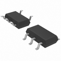
LT1615ES5-1#TRPBF Linear Technology, LT1615ES5-1#TRPBF Datasheet - Page 4

LT1615ES5-1#TRPBF
Manufacturer Part Number
LT1615ES5-1#TRPBF
Description
IC DC/DC CONV STEP-UP TSOT-23-5
Manufacturer
Linear Technology
Type
Step-Up (Boost)r
Datasheet
1.LT1615ES5TRMPBF.pdf
(8 pages)
Specifications of LT1615ES5-1#TRPBF
Internal Switch(s)
Yes
Synchronous Rectifier
No
Number Of Outputs
1
Voltage - Output
1.23 ~ 36 V
Current - Output
100mA
Voltage - Input
1 ~ 15 V
Operating Temperature
-40°C ~ 85°C
Mounting Type
Surface Mount
Package / Case
TSOT-23-5, TSOT-5, TSOP-5
Lead Free Status / RoHS Status
Lead free / RoHS Compliant
Power - Output
-
Frequency - Switching
-
Available stocks
Company
Part Number
Manufacturer
Quantity
Price
LT1615/LT1615-1
BLOCK DIAGRA
OPERATIO
The LT1615 uses a constant off-time control scheme to
provide high efficiencies over a wide range of output
current. Operation can be best understood by referring to
the block diagram in Figure 1. Q1 and Q2 along with R3 and
R4 form a bandgap reference used to regulate the output
voltage. When the voltage at the FB pin is slightly above
1.23V, comparator A1 disables most of the internal cir-
cuitry. Output current is then provided by capacitor C2,
which slowly discharges until the voltage at the FB pin
drops below the lower hysteresis point of A1 (typical
hysteresis at the FB pin is 8mV). A1 then enables the
internal circuitry, turns on power switch Q3, and the
current in inductor L1 begins ramping up. Once the switch
current reaches 350mA, comparator A2 resets the one-
shot, which turns off Q3 for 400ns. L1 then delivers
current to the output through diode D1 as the inductor
current ramps down. Q3 turns on again and the inductor
4
(EXTERNAL)
(EXTERNAL)
U
R1
R2
V
IN
V
OUT
W
FB
C1
3
* 12mV FOR LT1615-1
5
Q1
R5
40k
V
IN
Figure 1. LT1615 Block Diagram
Q2
X10
R6
40k
R3
30k
R4
140k
+
–
4
SHDN
A1
ONE-SHOT
ENABLE
400ns
current ramps back up to 350mA, then A2 resets the one-
shot, again allowing L1 to deliver current to the output.
This switching action continues until the output voltage is
charged up (until the FB pin reaches 1.23V), then A1 turns
off the internal circuitry and the cycle repeats. The LT1615
contains additional circuitry to provide protection during
start-up and under short-circuit conditions. When the FB
pin voltage is less than approximately 600mV, the switch
off-time is increased to 1.5 s and the current limit is
reduced to around 250mA (70% of its normal value). This
reduces the average inductor current and helps minimize
the power dissipation in the LT1615 power switch and in
the external inductor and diode. The LT1615-1 operates in
the same manner, except the switch current is limited to
100mA (the A2 reference voltage is 12mV instead of
42mV).
RESET
L1
A2
+
–
DRIVER
42mV*
1
Q3
0.12
SW
D1
2
GND
1615/-1 BD
C2
V
OUT
sn16151 16151fas


