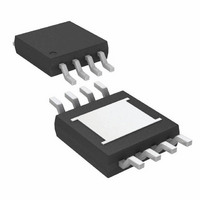
LT1961EMS8E Linear Technology, LT1961EMS8E Datasheet - Page 12

LT1961EMS8E
Manufacturer Part Number
LT1961EMS8E
Description
IC REG SW STEPUP 1.5A 8-MSOP
Manufacturer
Linear Technology
Type
Step-Up (Boost)r
Datasheet
1.LT1961EMS8E.pdf
(16 pages)
Specifications of LT1961EMS8E
Internal Switch(s)
Yes
Synchronous Rectifier
No
Number Of Outputs
1
Voltage - Output
1.2 ~ 35 V
Current - Output
1.5A
Frequency - Switching
1.25MHz
Voltage - Input
3 ~ 25 V
Operating Temperature
-40°C ~ 125°C
Mounting Type
Surface Mount
Package / Case
8-MSOP Exposed Pad, 8-HMSOP, 8-eMSOP
Lead Free Status / RoHS Status
Contains lead / RoHS non-compliant
Power - Output
-
Available stocks
Company
Part Number
Manufacturer
Quantity
Price
Company:
Part Number:
LT1961EMS8E
Manufacturer:
LINEAR
Quantity:
31
Part Number:
LT1961EMS8E
Manufacturer:
LINEAR/凌特
Quantity:
20 000
Part Number:
LT1961EMS8E#PBF
Manufacturer:
LINEAR/凌特
Quantity:
20 000
Company:
Part Number:
LT1961EMS8E#TRPBF
Manufacturer:
AMIS
Quantity:
6 218
Part Number:
LT1961EMS8E#TRPBF
Manufacturer:
LINEAR/凌特
Quantity:
20 000
LT1961
APPLICATIONS
THERMAL CALCULATIONS
Power dissipation in the LT1961 chip comes from four
sources: switch DC loss, switch AC loss, drive current, and
input quiescent current. The following formulas show how
to calculate each of these losses. These formulas assume
continuous mode operation, so they should not be used
for calculating efficiency at light load currents.
Switch loss:
R
Example: V
Total power dissipation = 0.23 + 0.31 + 0.07 + 0.005 =
0.62W
Thermal resistance for LT1961 package is influenced by
the presence of internal or backside planes. With a full
plane under the package, thermal resistance will be about
50°C/W. To calculate die temperature, use the appropriate
thermal resistance number and add in worst-case ambient
temperature:
If a true die temperature is required, a measurement of the
SYNC to GND pin resistance can be used. The SYNC pin
resistance across temperature must first be calibrated,
12
V
SW
IN
T
DC duty cycle
I
P
P
SW
SW
J
VIN
loss:
= Switch resistance (≈ 0.27Ω hot)
= T
,
=
=
=
A
(
(
V
DC I
+ θ
(
V
IN
OUT
IN SW
= 5V, V
JA
)(
V
)(
IN
)(
I
SW
50
(P
I
OUT
=
TOT
) (
U
)(
2
(
DC
OUT
)
R
V
)
OUT
SW
)
V
INFORMATION
= 12V and I
U
OUT
+
)
−
+
1
mA V
17
V
IN
n I
(
)
( )(
IN
SW
W
)
OUT
V
= 0.5A
OUT
)( )
U
f
with no device power, in an oven. The same measurement
can then be used in operation to indicate the die tempera-
ture.
FREQUENCY COMPENSATION
Loop frequency compensation is performed on the output
of the error amplifier (V
The main pole is formed by the series capacitor and the
output impedance (≈500kΩ) of the error amplifier. The
pole falls in the range of 2Hz to 20Hz. The series resistor
creates a “zero” at 1kHz to 5kHz, which improves loop
stability and transient response. A second capacitor, typi-
cally one-tenth the size of the main compensation capaci-
tor, is sometimes used to reduce the switching frequency
ripple on the V
voltage ripple attenuated by the output divider and multi-
plied by the error amplifier. Without the second capacitor,
V
To prevent irregular switching, V
kept below 50mV
maximum output load current and will also be increased if
poor quality (high ESR) output capacitors are used. The
addition of a 47pF capacitor on the V
ing frequency ripple to only a few millivolts. A low value for
R
may be inadequate.
C
C
V
V
g
R
V
pin ripple is:
will also reduce V
m
C
RIPPLE
OUT
C
Pin Ripple =
= Series resistor on V
= Error amplifier transconductance
(≈850μmho)
= DC output voltage
= Output ripple (V
C
pin. V
P–P
1.2(V
. Worst-case V
C
pin ripple, but loop phase margin
C
C
RIPPLE
pin ripple is caused by output
pin) with a series RC network.
(V
C
OUT
P–P
pin
)(g
)
C
)
m
C
C
pin ripple should be
)(R
pin ripple occurs at
pin reduces switch-
C
)
1961fa


