MCP1256-IMF Microchip Technology, MCP1256-IMF Datasheet - Page 11
MCP1256-IMF
Manufacturer Part Number
MCP1256-IMF
Description
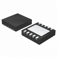
IC CHARGE PUMP DC/DC CONV 10DFN
Manufacturer
Microchip Technology
Type
Step-Up (Boost), Switched Capacitor (Charge Pump)r
Specifications of MCP1256-IMF
Internal Switch(s)
Yes
Synchronous Rectifier
No
Number Of Outputs
1
Voltage - Output
3.3V
Current - Output
100mA
Frequency - Switching
650kHz
Voltage - Input
1.8 ~ 3.6 V
Operating Temperature
-40°C ~ 125°C
Mounting Type
Surface Mount
Package / Case
10-DFN
For Use With
MCP1256/7/8/9EV - BOARD EVAL FOR MCP1256/7/8/9
Lead Free Status / RoHS Status
Lead free / RoHS Compliant
Power - Output
-


3.0
The descriptions of the pins are listed in Table 3-1.
TABLE 3-1:
3.1
3.1.1
MCP1256/8: PGOOD is high impedance when the out-
put voltage is in regulation. A logic low is asserted
when the output falls 7% (typical) below the nominal
value. The PGOOD output remains low until V
within 3% (typical) of its nominal value. On start-up, this
pin indicates when the output voltage reaches its final
value. PGOOD is high impedance when SHDN is low
or when BYPASS is low (MCP1258).
3.1.2
MCP1257/9: LBO is high impedance when the input
voltage is above the low-battery threshold voltage. A
logic low is asserted when the input falls below the low-
battery threshold voltage. The LBO output remains low
until V
the low-battery hysteresis voltage. LBO is high
impedance when SHDN is low or when BYPASS is low
(MCP1259).
3.2
3.2.1
MCP1256/7: A logic low signal applied to this pin
places the device into a SLEEP mode of operation. In
this mode, the device maintains regulation. SLEEP
mode performs pulse skip operation reducing the
current draw of the device at the expense of increased
output voltage ripple.
© 2006 Microchip Technology Inc.
DFN
10
1
2
3
4
5
6
7
8
9
IN
Pin No.
is above the low-battery threshold voltage plus
PIN DESCRIPTION
Status Indication (PGOOD, LBO)
Mode Selection (SLEEP, BYPASS)
POWER-GOOD OUTPUT PIN
(PGOOD)
LOW-BATTERY OUTPUT PIN (LBO)
ACTIVE LOW SLEEP MODE
(SLEEP)
MSOP
10
1
2
3
4
5
6
7
8
9
PIN FUNCTION TABLE
Symbol
BYPASS
PGOOD
SLEEP
SHDN
V
GND
LBO
C1+
C2+
C2-
C1-
V
OUT
IN
Power-Good Indication Open-Drain Output Pin: MCP1256 and MCP1258
Low-Battery Indication Open-Drain Output Pin: MCP1257 and MCP1259
Active Low SLEEP Mode Input Pin: MCP1256 and MCP1257
Active Low BYPASS Mode Input Pin: MCP1258 and MCP1259
Flying Capacitor Negative Pin
Flying Capacitor Positive Pin
Regulated 3.3V Output Voltage
Flying Capacitor Positive Pin
Power Supply Input Voltage
Flying Capacitor Negative Pin
0V Reference
Active Low SHUTDOWN Mode Input Pin
OUT
is
3.2.2
MCP1258/9: A logic low signal applied to this pin
places the device into a BYPASS mode of operation. In
this mode, the input supply voltage is connected
directly to the output.
3.3
A 1 μF ceramic flying capacitor is recommended.
3.4
A 1 μF ceramic flying capacitor is recommended.
3.5
Regulated 3.3V output. Bypass to GND with a
minimum of 2.2 μF.
3.6
A 1 μF ceramic flying capacitor is recommended.
3.7
A supply voltage of 1.8V to 3.6V is recommended.
Bypass to GND with a minimum of 1 μF.
3.8
A 1 μF ceramic flying capacitor is recommended.
3.9
Connect to negative terminal of and input supply.
3.10
A logic low signal applied to this pin disables the
device. A logic high signal applied to this pin allows
normal operation.
Flying Capacitor Negative (C2-)
Flying Capacitor Positive (C1+)
Regulated Output Voltage (V
Flying Capacitor Positive (C2+)
Power Supply Input Voltage (V
Flying Capacitor Negative (C1-)
0V Reference (GND)
Device Shut Down (SHDN)
Function
ACTIVE LOW BYPASS MODE
(BYPASS)
MCP1256/7/8/9
DS21989A-page 11
OUT
IN
)
)
Related parts for MCP1256-IMF
Image
Part Number
Description
Manufacturer
Datasheet
Request
R

Part Number:
Description:
BOARD EVAL FOR MCP1256/7/8/9
Manufacturer:
Microchip Technology
Datasheet:

Part Number:
Description:
IC CHARGE PUMP DC/DC CONV 10DFN
Manufacturer:
Microchip Technology
Datasheet:

Part Number:
Description:
IC CHARGE PUMP DC/DC CONV 10MSOP
Manufacturer:
Microchip Technology
Datasheet:
Part Number:
Description:
IC CHARGE PUMP DC/DC CONV 10MSOP
Manufacturer:
Microchip Technology
Datasheet:

Part Number:
Description:
Regulated 3.3V, Low-Ripple Charge Pump with Low-Operating Current SLEEP Mode or BYPASS Mode
Manufacturer:
Microchip Technology
Datasheet:
Part Number:
Description:
Low Noise positive Regulator pump w/low power SLEEP mode, -40C to +85C, 10-MSOP, TUBE
Manufacturer:
Microchip Technology
Datasheet:

Part Number:
Description:
MCP1,5 REC HSG10P
Manufacturer:
Tyco Electronics
Datasheet:


Part Number:
Description:
Manufacturer:
Microchip Technology Inc.
Datasheet:
Part Number:
Description:
Manufacturer:
Microchip Technology Inc.
Datasheet:
Part Number:
Description:
Manufacturer:
Microchip Technology Inc.
Datasheet:
Part Number:
Description:
Manufacturer:
Microchip Technology Inc.
Datasheet: